
FPGA Programming and Testing
Interactive Audio Lesson
Listen to a student-teacher conversation explaining the topic in a relatable way.
Introduction to Programming FPGAs
🔒 Unlock Audio Lesson
Sign up and enroll to listen to this audio lesson

Today, we're going to explore how to program an FPGA. Do any of you know what a configuration bitstream is?

Isn't it like a file that tells the FPGA how to behave?
Exactly! The configuration bitstream is crucial as it defines the logic implementation of your design. Can anyone tell me what tools are used to create this bitstream?

I think we can use Xilinx Vivado or Intel Quartus.
Great! Both tools help synthesize your design into a bitstream that programs the FPGA. Remember, we often refer to this process as programming the FPGA.

So, what happens after we create the bitstream?
Good question! After creating the bitstream, we need to load it into the FPGA. This step is critical to ensure our design works as intended.
In summary, programming FPGAs involves creating a configuration bitstream using tools like Vivado or Quartus and loading it onto the FPGA.
Testing FPGA Designs
🔒 Unlock Audio Lesson
Sign up and enroll to listen to this audio lesson

Now that we understand programming, let's discuss how we can test our FPGA designs effectively. What methods do you think we can use?
We can use LEDs and switches on a development board to check the outputs and inputs.
Exactly! Using LEDs allows us to visually monitor outputs. What about more complex signal analysis?

We can use logic analyzers to debug and verify signals.
Correct! Logic analyzers provide a powerful means to analyze signals precisely. Remember, thorough testing is key to verifying that our designs function correctly on real hardware.
To recap, we can test FPGA designs using development boards with LEDs and switches, as well as employing logic analyzers for deeper signal verification.
Verification of FPGA Functionality
🔒 Unlock Audio Lesson
Sign up and enroll to listen to this audio lesson
Verification is an essential part of FPGA development. Why do you think it's important to verify the functionality after loading the bitstream?
To ensure that our design works as we expected!
Exactly! Verification confirms that the programmed behavior aligns with the intended design. What could happen if we skip this step?
We might end up with errors in our output or even functional failures.
Right! So remember, verification is not something we can overlook. Always test and verify your designs post-programming.
In summary, after programming an FPGA, we must conduct thorough verification to ensure its functionality matches our design intentions, avoiding potential errors and failures.
Introduction & Overview
Read summaries of the section's main ideas at different levels of detail.
Quick Overview
Standard
The section outlines the steps required to program an FPGA with a generated configuration bitstream and emphasizes the importance of testing the system through various methods such as input monitoring on development boards. Key tools and techniques for successful verification are highlighted.
Detailed
FPGA Programming and Testing
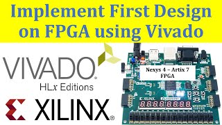
This section covers the essential processes for programming and testing FPGAs, which are critical steps in the FPGA development lifecycle. After designing a circuit and synthesizing it into a gate-level representation, tools like Xilinx Vivado and Intel Quartus help generate a configuration bitstream that configures the FPGA hardware. The programming process involves transferring this bitstream to the FPGA, ensuring that it is set up to perform the desired functions.
Once programmed, the next crucial step is testing, where the programmed design's functionality is verified. Various testing methods can be employed, including using development boards equipped with LEDs and switches to monitor inputs and outputs physically, or employing logic analyzers to observe the behavior of signals from the FPGA. These verification steps are essential to ensure that the design operates as intended, confirming both the functionality and performance of the system on hardware.
Youtube Videos
Audio Book
Dive deep into the subject with an immersive audiobook experience.
Configuration Bitstream Generation
Chapter 1 of 2
🔒 Unlock Audio Chapter
Sign up and enroll to access the full audio experience
Chapter Content
After synthesizing the design using tools like Xilinx Vivado or Intel Quartus, the configuration bitstream is generated.
Detailed Explanation
Once you have created and synthesized your design, the next step is to generate a configuration bitstream. This bitstream is a binary file that contains all the information needed by the FPGA to understand how to configure its logic blocks, routing resources, and I/O pins to implement the desired functionality of your design. Tools such as Xilinx Vivado or Intel Quartus are used to accomplish this step, making sure the design is ready for programming into the FPGA.
Examples & Analogies
Think of the configuration bitstream as a recipe for cooking. Just like a recipe tells you the steps, ingredients, and methods to produce a dish, the bitstream gives the FPGA the precise instructions for how to implement your design.
Programming the FPGA
Chapter 2 of 2
🔒 Unlock Audio Chapter
Sign up and enroll to access the full audio experience
Chapter Content
The FPGA is programmed with this bitstream file, and the system is verified by testing the inputs and monitoring the outputs on an FPGA development board using LEDs, switches, or a logic analyzer.
Detailed Explanation
After generating the configuration bitstream, the next step is to program the FPGA. This involves loading the bitstream into the FPGA device using specific programming tools or interfaces. Once the FPGA is programmed, you can verify the system's functionality by applying inputs, usually through development boards equipped with LEDs, switches, or other interactive components. Monitoring outputs allows you to ensure that the design works as intended and meets the original specifications.
Examples & Analogies
Imagine you’ve programmed a robot to perform certain tasks. After programming, you would physically test the robot's performance in its environment to see if it correctly executes the tasks as you intended. Similarly, after programming the FPGA, we test and monitor its behavior to confirm it functions correctly.
Key Concepts
-
Configuration Bitstream: A file that configures the FPGA according to the design specifications.
-
Development Board: A platform for physically testing and verifying FPGA behavior.
-
Logic Analyzer: A tool used to monitor and debug signals on the FPGA.
Examples & Applications
Using a development board with LEDs to visually test output signals from an FPGA design.
Employing a logic analyzer to monitor signal integrity and timing issues during FPGA operation.
Memory Aids
Interactive tools to help you remember key concepts
Rhymes
To program the FPGA with flair, make a bitstream, handle with care!
Stories
Imagine a chef programming a grill (the FPGA) with a recipe (the bitstream). Without checking the grill, the food may turn out wrong. After cooking, the chef tests the food to ensure it's delicious!
Memory Tools
To remember the FPGA programming process: 'PBT VLT' - Program, Bitstream, Test, Verify, Load, and Test.
Acronyms
FOR TEST
FPGA Output Review; Test Everything Systematically Tried.
Flash Cards
Glossary
- Configuration Bitstream
A binary file generated from the design that configures an FPGA to implement the desired functionalities.
- Programming
The process of loading a configuration bitstream into the FPGA hardware.
- Testing
The practice of verifying the functionality of an FPGA design after it has been programmed.
- Development Board
A physical board containing an FPGA along with input/output interfaces for testing and interaction.
- Logic Analyzer
An instrument used to capture and analyze digital signals from the FPGA for debugging purposes.
Reference links
Supplementary resources to enhance your learning experience.