Design and Implement Microfabrication Processes
Interactive Audio Lesson
Listen to a student-teacher conversation explaining the topic in a relatable way.
Overview of Microfabrication Process Flow
🔒 Unlock Audio Lesson
Sign up and enroll to listen to this audio lesson

Today, we're going to discuss the sequence of steps involved in microfabrication. Can anyone tell me what the first step is?

Is it substrate preparation?

That's correct! Substrate preparation is crucial as it sets the foundation for all subsequent processes. After that, what comes next?

Is it film deposition?

Yes! Film deposition layers the semiconductor materials. Throughout these stages, we need to consider yield and performance to ensure effectiveness.

What do we mean by yield?

Great question! Yield refers to the number of functional devices produced relative to what was attempted. It's critical for the economic viability of processes in microfabrication.

So, how do we maintain that yield through these steps?

It involves optimizing each process, from cleaning the substrates to ensuring uniform film thickness during deposition. Let’s review the complete flow next.

Okay, what comes after film deposition?

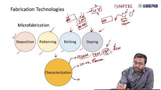
Next is patterning, followed by etching, doping, and finally packaging. Each step plays a meaningful role in producing high-quality devices.
Key Fabrication Techniques
🔒 Unlock Audio Lesson
Sign up and enroll to listen to this audio lesson

Let’s dive into specific techniques we use in microfabrication. Who can name one of them?

I think thin film deposition is one.

Exactly! Thin film deposition includes methods like PVD and CVD. Can anyone explain one of those methods briefly?

PVD stands for Physical Vapor Deposition, right?

Correct! It’s used to deposit thin films via sputtering. What do we know about the sputter yield?

The sputter yield is proportional to the ion energy divided by surface binding energy.

Perfect! Next is lithography. Can we talk about immersion lithography?

Is that the one that uses water to improve resolution?

That's right! It increases numerical aperture, allowing for smaller features. Who can summarize the importance of these techniques in the overall process?

They help ensure that each layer is properly formed and enhances device functionality!

Exactly. Techniques like advanced lithography are vital for achieving nodes less than 40nm.
Doping and Yield Optimization
🔒 Unlock Audio Lesson
Sign up and enroll to listen to this audio lesson

Let’s shift gears and discuss doping techniques today. Who knows what dopants are?

Aren't they materials added to modify electrical properties?

Absolutely! Techniques like ion implantation create specific dopant profiles. Can someone explain the Gaussian distribution in this context?

It shows how the dopant concentration decreases from the surface inward, based on the implant energy.

Good! Now, how do we ensure the maximum yield across all processes?

By monitoring defect density and controlling parameters statistically!

Exactly! Using Statistical Process Control to track these metrics is essential for optimizing yield.

That makes sense. If we can reduce defects, we increase yield, right?

Right! Defect density impacts yield significantly, as represented in the formula. Let’s summarize yield management strategies next.
Introduction & Overview
Read summaries of the section's main ideas at different levels of detail.
Quick Overview
Standard
In this section, the microfabrication process is thoroughly explored, outlining steps from substrate preparation to packaging. Key design rules and methodologies, along with critical fabrication techniques such as thin film deposition and lithography, are discussed to highlight their importance in ensuring yield and performance.
Detailed
Microfabrication is a multi-step process that converts raw semiconductor wafers into functional devices, involving careful consideration of each stage to maintain yield and device performance. It starts with substrate preparation, followed by film deposition, patterning, etching, doping, and finally packaging. The design methodology focuses on essential rules like minimum feature size and stacking compatibility, supported by tools like TCAD for simulation. Fabrication techniques such as PVD and CVD for deposition, advanced lithography methods (EUV and immersion), and etching processes are explored for their roles in achieving precision. Doping techniques, yield optimization strategies, emerging methods like 3D IC stacking, and real-world case studies underscore the complexity and advancements in microfabrication, ensuring robust device integration.
Youtube Videos


Audio Book
Dive deep into the subject with an immersive audiobook experience.
Overview of Process Flow
Chapter 1 of 3
🔒 Unlock Audio Chapter
Sign up and enroll to access the full audio experience
Chapter Content
2.1 Overview of Process Flow
- Definition:
- Structured sequence of steps to transform raw semiconductor wafers into functional devices.
- Key Stages:
- Substrate preparation → Film deposition → Patterning → Etching → Doping → Packaging
- Critical Consideration:
- Each step must maintain yield, uniformity, and device performance.
Detailed Explanation
The overview of process flow is about understanding how raw semiconductor wafers are transformed into devices we can use, like chips in our phones. This process is broken down into a series of steps: First, we prepare the substrate, which is the foundation. Next, we deposit films on the substrate, which form the various layers needed for the device. Then, we pattern these layers to create specific designs or circuits. After that, we etch away unwanted parts to refine the structure. Doping follows, where we introduce impurities to modify electrical properties. Finally, we package the devices to protect them and make them ready for use. It is crucial that each step is carefully managed to ensure high yield (number of usable products), uniform results across all devices, and optimal performance.
Examples & Analogies
Think of this process like baking a cake. You start with raw ingredients (the substrate), mix them (film deposition), pour them into a mold (patterning), bake them (etching), add frosting (doping for flavor), and finally package them nicely to serve at a party (packaging). Each step must be done correctly to ensure the cake tastes great and looks appealing!
Process Design Methodology
Chapter 2 of 3
🔒 Unlock Audio Chapter
Sign up and enroll to access the full audio experience
Chapter Content
2.2 Process Design Methodology
2.2.1 Design Rules
- Minimum Feature Size: Dictates lithography resolution (e.g., 7nm node).
- Alignment Tolerance: Mask-to-mask registration accuracy.
- Layer Stacking: Compatibility of materials (CTE matching).
Detailed Explanation
In this section, we focus on the design rules that guide the microfabrication process. The minimum feature size is crucial as it defines how small the intricate details on the semiconductor can be - for instance, a 7nm feature size means that we can make tiny components closer than this distance. Alignment tolerance is about ensuring that every layer or mask aligns perfectly with the ones below it, which is critical for the function of the final device. Lastly, layer stacking looks at the compatibility of materials. Different materials expand and contract at different rates (this is called Coefficient of Thermal Expansion, or CTE), so we have to ensure that when they are layered, they don't cause issues as temperature changes.
Examples & Analogies
Consider building a house. The minimum feature size is like deciding how big the bricks can be. If they're too small, it takes longer to build. Alignment tolerance is like ensuring that each wall lines up perfectly with the roof – if it's off, the structure won't be stable. Layer stacking is about making sure that the materials used (like wood and brick) can work together without cracking when temperatures change.
Process Simulation
Chapter 3 of 3
🔒 Unlock Audio Chapter
Sign up and enroll to access the full audio experience
Chapter Content
2.2.2 Process Simulation
- Tools:
- TCAD (Technology Computer-Aided Design) for virtual prototyping.
- Examples: Silvaco Athena, Sentaurus Process.
Detailed Explanation
Now we look at process simulation, which uses tools like TCAD (Technology Computer-Aided Design) to create virtual models of how the microfabrication processes would operate. This allows engineers to test design principles and make adjustments without having to produce actual physical devices, saving time and resources. Tools like Silvaco Athena and Sentaurus Process provide sophisticated simulations that can predict outcomes based on variables such as material properties and process parameters.
Examples & Analogies
Think of it as creating a video game before building the real world. Game designers can simulate various environments, characters, and scenarios on a computer. They can see how things would function, catch problems, and modify anything before putting in the resources to develop a real game.
Key Concepts
-
Microfabrication Process Flow: The structured sequence of steps to convert semiconductor wafers into devices.
-
Doping Techniques: Methods used to modify the electrical properties of semiconductors.
-
Yield Optimization: Strategies to enhance the number of usable devices produced in fabrication.
Examples & Applications
In CMOS fabrication, the process involves well formation, gate oxide deposition, and source/drain implantation, culminating in device assembly.
In MEMS process flows, surface micromachining often includes sacrificial layer etching to create micromechanical structures.
Memory Aids
Interactive tools to help you remember key concepts
Rhymes
To make devices that will work, substrate prep is the first perk!
Stories
Imagine a sculptor carving a statue; the substrate is the block, the layers are the chiseling to bring the final shape into reality.
Memory Tools
S-P-E-D-P: Substrate, Patterning, Etching, Doping, Packaging - remember the process flow steps!
Acronyms
PEEL
Preparation
Etching
Evaluation
Layering - key phases in microfabrication.
Flash Cards
Glossary
- Doping
The process of adding impurities to semiconductor materials to modify their electrical properties.
- Yield
The proportion of functional devices obtained from a fabrication process relative to the total number attempted.
- Thin Film Deposition
A technique to deposit thin layers of material onto a substrate.
- Lithography
A process used to transfer patterns onto a substrate, essential for defining the geometry of devices.
Reference links
Supplementary resources to enhance your learning experience.
