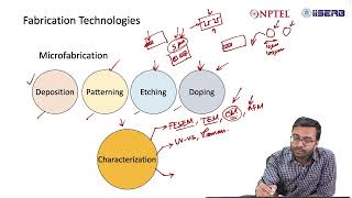
Thin Film Deposition
Interactive Audio Lesson
Listen to a student-teacher conversation explaining the topic in a relatable way.
Introduction to Thin Film Deposition
🔒 Unlock Audio Lesson
Sign up and enroll to listen to this audio lesson

Today, we will explore thin film deposition, a foundational technique in microfabrication processes. Why do you think adding thin layers of materials is essential?

I think it’s important for controlling the properties of semiconductor devices?

And to create different functionalities on the same chip!

Exactly! Thin films allow us to engineer electrical, optical, and mechanical properties in materials essential for the device's overall function.
Physical Vapor Deposition (PVD)
🔒 Unlock Audio Lesson
Sign up and enroll to listen to this audio lesson

Let’s discuss Physical Vapor Deposition, specifically sputtering. Can anyone explain what sputtering involves?

Isn’t it when ions hit a target material and eject atoms from it?

Correct! The sputter yield describes this process and is expressed as Y proportional to E over U₀. What do E and U₀ represent?

E is ion energy and U₀ is the binding energy of the atoms at the surface, right?

That’s right! Higher ion energy typically increases the sputter yield, which ultimately affects the film's deposition rate and quality.
Chemical Vapor Deposition (CVD)
🔒 Unlock Audio Lesson
Sign up and enroll to listen to this audio lesson

Now, let’s look at Chemical Vapor Deposition or CVD. Can anyone name some types of CVD?

There’s LPCVD and PECVD!

Great. What benefits do you think LPCVD provides?

It offers uniform step coverage?

Exactly! And what about PECVD?

It can operate at lower temperatures!

Correct. Understanding these variants helps us choose the right method for specific applications in microfabrication.
Application of Thin Film Techniques
🔒 Unlock Audio Lesson
Sign up and enroll to listen to this audio lesson

Let’s talk about real-world applications. Can anyone give me an example of where thin film deposition techniques are critical?

In making transistors or solar cells!

Absolutely! Thin films are essential for isolating components and ensuring they function correctly. Why do uniformity and quality matter here?

If the films aren’t uniform, it can lead to defects and poor performance!

That's right! Consistency in film characteristics is key to achieving high performance and yield in microfabricated devices.
Introduction & Overview
Read summaries of the section's main ideas at different levels of detail.
Quick Overview
Standard
In this section, we explore thin film deposition techniques essential for microfabrication processes. It discusses PVD (sputtering) and its foundational principles, as well as CVD methods such as LPCVD and PECVD, which are indispensable for achieving desired film properties in semiconductor devices.
Detailed
Thin film deposition is a vital process in semiconductor manufacturing that entails adding thin layers of materials to a substrate. This section focuses on two main techniques: Physical Vapor Deposition (PVD), specifically sputtering, and Chemical Vapor Deposition (CVD). PVD involves the transfer of material through physical processes, yielding layers with great precision. Sputtering is governed by the equation for sputter yield, emphasizing the relationship between ion energy and surface binding energy, influencing the quality of the films produced. Meanwhile, CVD encompasses two popular variants: Low Pressure Chemical Vapor Deposition (LPCVD), which promotes uniform coverage, and Plasma Enhanced Chemical Vapor Deposition (PECVD), allowing growth at lower temperatures. Understanding these methods is critical for developing advanced devices, where film properties directly impact device performance and yield.
Youtube Videos


Audio Book
Dive deep into the subject with an immersive audiobook experience.
Physical Vapor Deposition (PVD)
Chapter 1 of 2
🔒 Unlock Audio Chapter
Sign up and enroll to access the full audio experience
Chapter Content
PVD (Sputtering):
- Equation: Sputter yield \( Y \propto \frac{E}{U_0} \) (E=ion energy, U₀=surface binding energy).
Detailed Explanation
Physical Vapor Deposition, commonly referred to as PVD, is a vacuum deposition method used to produce thin films. One specific type of PVD is sputtering, where energetic ions strike a target material, ejecting atoms that then deposit on a substrate. The sputter yield equation \( Y \propto \frac{E}{U_0} \) illustrates this process, where \( E \) represents the energy of the ions striking the surface, and \( U_0 \) represents the energy needed to release an atom from the target. Higher ion energies result in higher sputter yields.
Examples & Analogies
Imagine playing billiards where a cue ball (the ions) strikes the balls on the table (the target material). The harder you strike, the more likely you are to knock balls off the table (eject atoms). The energy you apply to the cue ball corresponds to the ion energy in sputtering.
CVD Variants
Chapter 2 of 2
🔒 Unlock Audio Chapter
Sign up and enroll to access the full audio experience
Chapter Content
CVD Variants:
- LPCVD (Low Pressure): Uniform step coverage.
- PECVD (Plasma Enhanced): Low-temperature deposition.
Detailed Explanation
Chemical Vapor Deposition (CVD) is another method for creating thin films, where gaseous chemical precursors react and deposit on a substrate to form solid films. There are variants such as LPCVD (Low Pressure CVD), which operates under reduced pressure to provide more uniform film coverage over complex geometries. Another variant is PECVD (Plasma Enhanced CVD), which uses plasma to enhance chemical reactions, allowing deposition at lower temperatures, which is beneficial for temperature-sensitive substrates or materials.
Examples & Analogies
Think of CVD as baking a cake: in LPCVD, you use a special pan that ensures even heat distribution for an evenly baked cake, while in PECVD, you use a quicker cooking method (like a microwave) that works well even if your ingredients are delicate.
Key Concepts
-
Thin Film Deposition: Refers to applying a thin layer of material, vital for microfabrication.
-
PVD (Sputtering): A method of depositing materials through the action of energetic ions.
-
CVD: Utilizes gaseous chemicals to form solid films, critical for semiconductor manufacturing.
Examples & Applications
Sputtering is used in depositing metals for interconnects in ICs.
LPCVD is commonly used for depositing silicon nitride layers in semiconductor devices.
Memory Aids
Interactive tools to help you remember key concepts
Rhymes
In the lab, thin films go pop, PVD and CVD, never stop!
Stories
Imagine a painter who, instead of using a brush, uses tiny particles carried by the wind to paint layers on a wall. This is akin to sputtering in PVD.
Memory Tools
PVD = Paint with Vapor Drops. CVD = Chemical to Vaporize Deposits.
Acronyms
CVD
Create Visibility Dynamically (for film coverage)!
Flash Cards
Glossary
- Thin Film Deposition
The process of applying a very thin layer of material onto a substrate.
- Physical Vapor Deposition (PVD)
A vacuum deposition method where material is deposited in vapor form and then condensed on the substrate.
- Sputtering
A PVD method where energy from ions is used to eject atoms from a target material.
- Chemical Vapor Deposition (CVD)
A process where gaseous reactants are used to create a solid material on a substrate.
- LPCVD
Low Pressure Chemical Vapor Deposition; used for uniform film deposition.
- PECVD
Plasma Enhanced Chemical Vapor Deposition; enables low-temperature film growth.
Reference links
Supplementary resources to enhance your learning experience.
