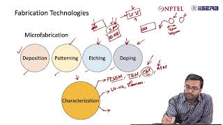
Overview of Process Flow
Interactive Audio Lesson
Listen to a student-teacher conversation explaining the topic in a relatable way.
Understanding Substrate Preparation
🔒 Unlock Audio Lesson
Sign up and enroll to listen to this audio lesson

Let's start by discussing substrate preparation. Why do you think it's essential to have a clean and prepared substrate before the fabrication process begins?

I think it’s to ensure that the materials will adhere properly and the devices will work correctly.

Exactly! A clean substrate is crucial for preventing defects, which can impact yield. Can anyone remember what can happen if the substrate isn't prepared correctly?

Oh, it can lead to contamination and defects in the final product, right?

Yes! Remember, 'Clean starts the scene!' It's a good way to recall that cleaning impacts the outcome significantly. Now, what materials do we commonly use as substrates?

Silicon is a common one, isn't it?

Correct! Silicon is indeed the most widely used substrate material. Let's summarize: Substrate preparation is crucial for cleanliness and integrity before moving on to film deposition.
Exploring Film Deposition Techniques
🔒 Unlock Audio Lesson
Sign up and enroll to listen to this audio lesson

After substrate preparation, we move to film deposition. Can anyone name different deposition techniques?

I've heard of Chemical Vapor Deposition and Physical Vapor Deposition.

Exactly! Let's remember these as CVD and PVD. Why do you think we have different techniques?

Probably because each has its advantages for specific materials or purposes?

Right! Each method offers unique benefits, for example, CVD provides excellent uniformity, whereas PVD might be better for certain materials. Can you think of a scenario where one might be preferred over the other?

I think CVD might be used for making thin films over complicated geometries, right?

Absolutely! Understanding when to use each technique is crucial. Let's summarize: Film deposition techniques are essential for creating usable layers and must be chosen based on desired outcomes.
The Role of Doping
🔒 Unlock Audio Lesson
Sign up and enroll to listen to this audio lesson

Now, let’s talk about doping. What is doping in the context of semiconductor fabrication?

Is it like adding impurities to change the electrical properties?

Exactly! Doping introduces elements that either increase or decrease the number of free charge carriers. Can someone provide an example of a dopant?

Phosphorus is often used to create n-type semiconductors, isn't it?

Yes! You’re on the right track! Remember, ‘P for Phosphorus means Positive flow for n-type.’ Doping is vital as it defines the functionality of the devices. Any questions before we summarize?

How does doping affect the yield?

Excellent question! Doping needs to be controlled precisely; otherwise, it might lead to device failures which decrease yield. Doping is crucial for device performance. Let’s recap: Doping alters electrical properties and must be precisely managed.
Introduction & Overview
Read summaries of the section's main ideas at different levels of detail.
Quick Overview
Standard
The Overview of Process Flow outlines the critical stages involved in semiconductor fabrication, highlighting substrate preparation, film deposition, patterning, etching, doping, and packaging as essential steps while emphasizing the importance of yield and device performance.
Detailed
Overview of Process Flow
The Overview of Process Flow outlines the comprehensive approach to converting raw semiconductor wafers into fully operational devices through a series of structured stages. The primary stages include:
1. Substrate Preparation: Ensuring that the semiconductor wafer is clean and free of contaminants.
2. Film Deposition: Various materials are deposited onto substrate surfaces to create functional layers.
3. Patterning: Applying specific patterns to these layers through photolithography.
4. Etching: Removing excess material to define the device structures.
5. Doping: Introducing impurities to modify electrical properties.
6. Packaging: Protecting and connecting the final device for use.
A critical aspect of each stage is to maintain high yield, uniformity, and optimum device performance, which are vital for the efficiency and cost-effectiveness of semiconductor device manufacturing.
Youtube Videos


Audio Book
Dive deep into the subject with an immersive audiobook experience.
Definition of Process Flow
Chapter 1 of 3
🔒 Unlock Audio Chapter
Sign up and enroll to access the full audio experience
Chapter Content
- Definition:
- Structured sequence of steps to transform raw semiconductor wafers into functional devices.
Detailed Explanation
The definition of process flow refers to a systematic series of actions that convert raw materials, specifically semiconductor wafers, into functional electronic devices. Each step in the sequence is crucial for ensuring that the final product meets the required specifications and performance standards.
Examples & Analogies
Think of process flow like a recipe in cooking: you have raw ingredients (like semiconductor wafers) that you follow specific steps with (mixing, baking, cooling), to ultimately create a delicious dish (functional device). Just as skipping or altering steps can ruin a recipe, missing steps in process flow can lead to defective devices.
Key Stages of Process Flow
Chapter 2 of 3
🔒 Unlock Audio Chapter
Sign up and enroll to access the full audio experience
Chapter Content
- Key Stages:
- Substrate preparation → Film deposition → Patterning → Etching → Doping → Packaging
Detailed Explanation
The key stages in the process flow represent a sequential approach to microfabrication. Each stage serves a distinct purpose:
1. Substrate Preparation: Prepares the wafer surface for further processing.
2. Film Deposition: Adds thin layers of materials onto the wafer for various functions.
3. Patterning: Defines specific areas on the wafer where additional processes will occur.
4. Etching: Removes unwanted material to create the desired patterns.
5. Doping: Introduces impurities into the semiconductor to modify its electrical properties.
6. Packaging: Encases the finished device for protection and integration into electronic systems.
Examples & Analogies
Consider building a house. You start by preparing the land (substrate preparation), then build the framework (film deposition), outline the rooms (patterning), remove excess materials (etching), add electrical wiring (doping), and finally, decorate and furnish (packaging) to create a functional home.
Critical Considerations
Chapter 3 of 3
🔒 Unlock Audio Chapter
Sign up and enroll to access the full audio experience
Chapter Content
- Critical Consideration:
- Each step must maintain yield, uniformity, and device performance.
Detailed Explanation
In the microfabrication process, it is essential that each step is executed with precision to maintain three critical parameters:
1. Yield: The quantity of good devices produced from a batch should be maximized.
2. Uniformity: All wafers and devices should exhibit consistent characteristics to ensure reliability.
3. Device Performance: Each device should function as intended, meeting electrical and physical specifications.
Examples & Analogies
Think of a factory producing light bulbs. If some bulbs burn out faster than others (poor yield), if their brightness varies (lack of uniformity), or if they fail to light up at all (device performance issues), customers will be dissatisfied. Similarly, in microfabrication, high standards in these areas are crucial for industry success.
Key Concepts
-
Substrate Preparation: Essential for ensuring good adherence and defect-free surfaces.
-
Film Deposition: Various techniques deposit materials, influencing the performance of devices.
-
Doping: Critical for achieving desired electrical properties.
-
Yield: A measure of successful device fabrication.
-
Etching: Pattern generation that defines the physical features of devices.
Examples & Applications
Silicon wafers are frequently used substrates due to their excellent semiconductor properties.
Chemical Vapor Deposition is often applied to deposit silicon dioxide layers on semiconductor substrates.
Memory Aids
Interactive tools to help you remember key concepts
Rhymes
Start with prep, to avoid a mishap, clean is the key, for yield to be snappy!
Stories
Once there was a silicon wafer that wanted to be a great semiconductor. It knew that if it didn't get cleaned thoroughly, its story would end before it even began—hurdling into defects, it would be lost among failed devices!
Memory Tools
Remember these stages: S, F, P, E, D, P for Substrate, Film, Patterning, Etching, Doping, Packaging.
Acronyms
SP-FEDP to remember the key stages of semiconductor processing
Substrate Preparation
Film deposition
Patterning
Etching
Doping
Packaging.
Flash Cards
Glossary
- Substrate Preparation
The process of preparing semiconductor wafers by ensuring they are clean and free of contaminants.
- Film Deposition
Methods used to deposit thin films of materials onto substrates in semiconductor fabrication.
- Doping
The introduction of impurities into a semiconductor to alter its electrical properties.
- Yield
The ratio of functional devices produced to the total number of devices fabricated.
- Etching
The process of removing material from the surface of a semiconductor to create patterns.
Reference links
Supplementary resources to enhance your learning experience.
