
Key Fabrication Techniques
Interactive Audio Lesson
Listen to a student-teacher conversation explaining the topic in a relatable way.
Thin Film Deposition
🔒 Unlock Audio Lesson
Sign up and enroll to listen to this audio lesson

Today, we are diving into thin film deposition techniques, starting with Physical Vapor Deposition or PVD. Can anyone tell me what this involves?

Isn't that where atoms are deposited from a vapor onto a surface?
Exactly! One common method under PVD is sputtering. The efficiency of this process can be described with the formula regarding sputter yield. Can anyone share what affects the sputter yield?

I think it’s the ion energy and surface binding energy.
Correct! The equation shows that sputter yield (Y) increases with more ion energy. Now, let’s compare that with Chemical Vapor Deposition or CVD. What are some variations of CVD?

There’s LPCVD and PECVD!
Good job! LPCVD is known for its uniform coverage, while PECVD allows low-temperature processing. I remember that by the phrase 'Low Pressure, Cooling Down for PECVD.' Overall, thin film deposition is crucial for forming transistor channels in microfabrication.
In summary, PVD involves physical methods like sputtering, while CVD uses chemical reactions to form thin films. Both are vital!
Advanced Lithography
🔒 Unlock Audio Lesson
Sign up and enroll to listen to this audio lesson

Shifting our focus, let's explore advanced lithography. Who can explain what immersion lithography is?
That’s when water is used between the lens and the wafer to improve resolution!
Absolutely right! It increases the numerical aperture, allowing for finer resolutions—below 40nm. Now, what about Extreme Ultraviolet lithography? Why is it important?
It allows for the production of features smaller than 7nm, which is essential for new devices!
Exactly! Remember that EUV operates at 13.5nm wavelengths. Imagine how that impacts our modern devices. Can someone recall the purpose of these advanced lithography techniques?

They help create the intricate patterns needed in semiconductor devices!
Right again! In summary, immersion lithography enhances resolution, and EUV lithography paves the way for the next generation of problem-solving microelectronics!
Etching Processes
🔒 Unlock Audio Lesson
Sign up and enroll to listen to this audio lesson
Now let’s tackle etching processes, another key area in microfabrication! What can you tell me about Deep Reactive Ion Etching?
It’s a method that creates high-aspect-ratio features?
Correct! The Bosch process alternates between etching and passivation, crucial for creating trenches. Can someone remind us what selectivity metrics refer to in etching?
It’s the ratio of etching rates between the film and the mask, right?
Exactly! The equation for selectivity is key: S equals the etch rate of the film divided by the etch rate of the mask. Why do we care about selectivity?
It helps to ensure that the patterned areas are etched accurately without affecting the mask.
Great point! To sum up, DRIE and selectivity are vital for ensuring that we achieve the desired microstructures without damaging underlying layers.
Introduction & Overview
Read summaries of the section's main ideas at different levels of detail.
Quick Overview
Standard
In this section, we explore critical fabrication techniques, focusing on thin film deposition methods such as PVD and CVD, advanced lithography techniques like immersion lithography and EUV, as well as fundamental etching processes necessary for producing high-precision microdevices. Understanding these techniques is vital for the successful implementation of microfabrication processes.
Detailed
Key Fabrication Techniques in Microfabrication
This section delves into the fundamental techniques used in microfabrication, which are pivotal for transforming designs into functional semiconductor devices. The techniques discussed include:
Thin Film Deposition
- Physical Vapor Deposition (PVD): Specifically, sputtering is highlighted, where the sputter yield is influenced by the ion energy (E) in relation to the surface binding energy (U₀). This technique is critical for creating thin films on semiconductor substrates.
- Chemical Vapor Deposition (CVD): Various types such as LPCVD (Low Pressure) and PECVD (Plasma Enhanced) are detailed. LPCVD is favored for its uniform step coverage, while PECVD allows for low-temperature processes, vital for certain material applications.
Advanced Lithography
- Immersion Lithography: Utilizing water to increase numerical aperture (NA), this technique enables resolution capabilities below 40nm, thus playing a critical role in creating intricate patterns on chip surfaces.
- Extreme Ultraviolet Lithography (EUV): Operating at a wavelength of 13.5nm, EUV is essential for producing features smaller than 7nm, making it a cornerstone technology for the next generation of semiconductor devices.
Etching Processes
- Deep Reactive Ion Etching (DRIE): The Bosch process is a classic example, where alternating etch and passivation cycles allow for the realization of high-aspect-ratio features, crucial in microelectromechanical systems (MEMS).
- Selectivity Metrics: The etch rate is measured with a focus on the selectivity ratio, which determines the etching effectiveness relative to the masking materials.
Understanding these techniques offers insights into their practical applications and significance in advancing microfabrication processes.
Youtube Videos


Audio Book
Dive deep into the subject with an immersive audiobook experience.
Thin Film Deposition
Chapter 1 of 3
🔒 Unlock Audio Chapter
Sign up and enroll to access the full audio experience
Chapter Content
2.3.1 Thin Film Deposition
- PVD (Sputtering):
- Equation: Sputter yield \( Y \propto \frac{E}{U_0} \) (E=ion energy, U₀=surface binding energy).
- CVD Variants:
- LPCVD (Low Pressure): Uniform step coverage.
- PECVD (Plasma Enhanced): Low-temperature deposition.
Detailed Explanation
Thin Film Deposition involves applying a very thin layer of material on a substrate. Two primary methods include Physical Vapor Deposition (PVD) and Chemical Vapor Deposition (CVD). In PVD, sputtering is a technique where ions hit a target material (the source), dislodging atoms that then settle onto the substrate. The efficiency of sputtering is described by the sputter yield equation, which measures how effectively atoms are ejected from the target based on ion energy and surface binding energy. CVD, on the other hand, uses gaseous reactants to produce thin films through chemical reactions. LPCVD is important for achieving uniform coverage, especially on complex shapes, while PECVD allows for deposition at lower temperatures, making it suitable for sensitive materials.
Examples & Analogies
Think of PVD like using a spray can: just as you spray paint onto a surface to create a color layer, PVD deposits materials onto a substrate. Meanwhile, CVD is akin to cooking a dish where ingredients (gases) react and create the final meal (thin film) as it bakes together in an oven!
Advanced Lithography
Chapter 2 of 3
🔒 Unlock Audio Chapter
Sign up and enroll to access the full audio experience
Chapter Content
2.3.2 Advanced Lithography
- Immersion Lithography:
- Uses water to increase NA (Resolution < 40nm).
- Extreme UV (EUV):
- 13.5nm wavelength for <7nm nodes.
Detailed Explanation
Advanced lithography techniques are critical for defining patterns on semiconductor wafers. Immersion lithography enhances resolution by using a liquid (often water) between the lens and the wafer, increasing the numerical aperture (NA) and hence allowing for smaller features—down to 40nm. Extreme UV lithography further pushes this boundary with a laser light source operating at a wavelength of 13.5nm, enabling the fabrication of devices at nodes smaller than 7nm, an essential requirement for modern high-performance chips.
Examples & Analogies
Imagine you're trying to take a clear photograph of a small object. If you have a regular camera (standard lithography), you might capture a decent image, but if you switch to a high-powered microscope (immersion lithography), you'll see even finer details. Now, using a cutting-edge optical lens that can capture the smallest details in microscopic petals (EUV) allows you to reveal features that are virtually unseeable with regular means.
Etching Processes
Chapter 3 of 3
🔒 Unlock Audio Chapter
Sign up and enroll to access the full audio experience
Chapter Content
2.3.3 Etching Processes
- Deep RIE (Bosch Process):
- Alternating SF₆ etch and C₄F₆ passivation cycles for high-aspect-ratio trenches.
- Selectivity Metrics:
- \( S = \frac{Etch\ Rate_{film}}{Etch\ Rate_{mask}} \).
Detailed Explanation
Etching processes are used to remove material selectively from a substrate, allowing for the patterning of intricate designs. The Deep Reactive Ion Etching (Bosch Process) utilizes alternating cycles of sulfur hexafluoride (SF₆) for etching and carbon tetrafluoride (C₄F₆) for passivation, creating deep and narrow trenches essential for modern devices. The selectivity metrics determine how effectively different materials can be etched while preserving others, an important aspect in ensuring the desired features are achieved without damaging underlying structures.
Examples & Analogies
Imagine sculpturing stone where you want to create a tall, thin statue. The Bosch Process is like taking chisels of different shapes to carve out deep details without affecting the integrity of surrounding stone; it's about precision and ensuring every cut counts without flaking away other areas.
Key Concepts
-
Thin Film Deposition: Techniques such as PVD and CVD for creating layers of materials.
-
Advanced Lithography: High-precision techniques allowing the creation of intricate micropatterns.
-
Etching Processes: Essential methods for material removal and feature definition in microfabrication.
Examples & Applications
Using LPCVD to deposit silicon nitride coatings in semiconductor applications.
Employing immersion lithography to fabricate the latest smartphone chips.
Memory Aids
Interactive tools to help you remember key concepts
Rhymes
In film deposition, don’t be shy, choose PVD or CVD to fly high!
Stories
Imagine a scientist named Dr. Litho who used the magic of immersion water to create patterns as sharp as a knife's edge in semicond
Memory Tools
//www.youtube.com/watch?v=lRCG1dNMhrw" target="_blank">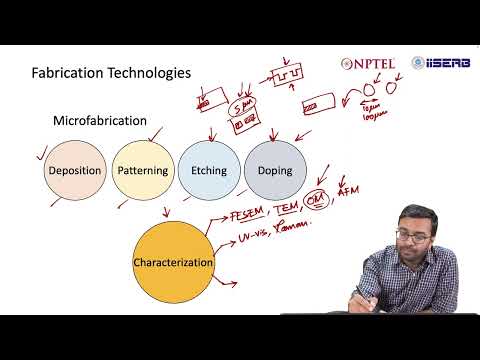
Microfabrication Technologies
Memory Tools
//img.youtube.com/vi/91qJw1LPRr8/0.jpg" alt="Introduction to Microfabrication" style="width:300px;"/>
Introduction to Microfabricationuctor chips.
Memory Tools
Remember PVD and CVD with the phrase: 'Physical Fun, Chemical Run'.
Acronyms
LITHE for lithography
for Light
for Immersion
for Techniques
for High Resolution
for Essential.
Flash Cards
Glossary
- PVD (Physical Vapor Deposition)
A technique for depositing thin films by physical means, such as sputtering.
- CVD (Chemical Vapor Deposition)
A process where thin films are deposited using chemical reactions.
- Immersion Lithography
A lithography technique that uses a liquid medium to achieve high-resolution patterns.
- EUV (Extreme Ultraviolet Lithography)
A next-generation lithography technique using extreme ultraviolet light for deep sub-7nm patterning.
- Deep Reactive Ion Etching (DRIE)
An etching method that creates high-aspect-ratio features using alternating etching and passivation.
- Selectivity Metrics
Measurements that determine the effectiveness of etching rates between different materials.
Reference links
Supplementary resources to enhance your learning experience.