
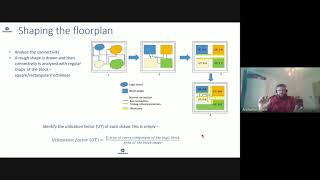
Area Optimization
Interactive Audio Lesson
Listen to a student-teacher conversation explaining the topic in a relatable way.
Introduction to Area Optimization
🔒 Unlock Audio Lesson
Sign up and enroll to listen to this audio lesson

Welcome class! Today, we are diving into area optimization in VLSI design. Can anyone tell me why optimizing the area of a chip is important?

I think it's about fitting all the components into the chip space properly!
Exactly! Efficiently using the available chip surface is crucial for performance and manufacturability. This leads us to techniques like cell resizing. Who can explain what cell resizing is?

It’s when we change the size of cells to make them fit better, right?
Right! Remember, we have to maintain timing and power constraints while doing this. Let's move on to block merging!
Cell Resizing
🔒 Unlock Audio Lesson
Sign up and enroll to listen to this audio lesson

Cell resizing helps optimize area by modifying dimensions. Why do we do this?

To reduce the chip size while keeping it efficient!
Correct! It’s a balancing act. We need to ensure that the resizing does not affect performance negatively. What’s the trade-off we might face?

Potentially increased power consumption if we make cells too small!
Excellent point! Remember, power and area often have inverse relationships. Let’s move to block merging next.
Block Merging
🔒 Unlock Audio Lesson
Sign up and enroll to listen to this audio lesson
Block merging combines smaller functions into a larger one, saving area. Can someone explain why this is beneficial?
It reduces the number of blocks, which makes routing simpler!
Exactly. Fewer blocks mean reduced routing complexity and risk of errors. Can you think of an example of where this might be applied?
In memory controllers, merging smaller data processing units could help.
Absolutely! Let’s now discuss wirelength minimization strategies.
Wirelength Minimization
🔒 Unlock Audio Lesson
Sign up and enroll to listen to this audio lesson
Minimizing wirelength is key to performance improvement as it decreases delay. Why might it be important to keep cells that interact close together?
It minimizes the wire length, which reduces capacitance and delays!
Correct again! Proximity matters for efficiency. This technique is interlinked with both timing and area considerations.
So, it’s like a web—we should keep related cells closely knit?
That’s a great analogy! Remember, optimizing area can lead to better overall chip performance.
Summary and Key Takeaways
🔒 Unlock Audio Lesson
Sign up and enroll to listen to this audio lesson
To wrap up, we’ve learned about cell resizing, block merging, and wirelength minimization as strategies for area optimization. Why is it essential to consider area optimization in chip design?
It contributes to better performance while managing power and space!
And it helps ensure manufacturability of the design!
Absolutely! Well done, everyone. Remember these concepts as you work on your own designs!
Introduction & Overview
Read summaries of the section's main ideas at different levels of detail.
Quick Overview
Standard
Area optimization is a crucial aspect of VLSI chip design, where methods like cell resizing, block merging, and wirelength minimization are applied to efficiently use chip space. These strategies aim to enhance the overall performance of the chip while maintaining power and timing constraints.
Detailed
Area Optimization
In the field of VLSI design, optimizing the area of a chip is vital for ensuring that the final product does not exceed spatial constraints while still delivering high performance. Several techniques are employed to achieve this goal:
Key Techniques
- Cell Resizing: This technique involves adjusting the dimensions of standard cells without violating timing and power specifications. By making cells smaller or larger, designers can influence the overall die size and the placement of cells within the layout.
- Block Merging: Smaller functional blocks can be combined into larger blocks to reduce the number of separate entities that need to be routed. This method can lead to significant area savings and can simplify the layout as interconnect complexity decreases.
- Wirelength Minimization: A fundamental strategy to optimize chip area involves arranging related cells nearby. This proximity reduces the length of the wires needed for interconnections, thereby minimizing delay due to capacitance and enhancing speed.
Significance
Each of these techniques requires careful consideration of trade-offs between performance, power consumption, and manufacturability. As chip designs become increasingly complex, efficient area optimization plays a crucial role in the successful development of VLSI chips, ensuring that they are not only functional but also compact and efficient.
Youtube Videos


Audio Book
Dive deep into the subject with an immersive audiobook experience.
Cell Resizing
Chapter 1 of 3
🔒 Unlock Audio Chapter
Sign up and enroll to access the full audio experience
Chapter Content
● Cell Resizing: Modifying the size of cells to optimize chip area while maintaining timing and power constraints.
Detailed Explanation
Cell resizing refers to the process of changing the dimensions of the individual cells within a chip design. The main goal is to make better use of the available area on the chip. By adjusting the sizes of the cells, designers can fit more cells into the same amount of space, which can lead to a smaller overall chip area. However, it’s important to ensure that resizing does not negatively affect the chip’s performance, such as maintaining the timing of signals and keeping power consumption within desired limits.
Examples & Analogies
Think of cell resizing like rearranging furniture in a small apartment. If you have a sofa that’s too large, you might need to swap it for a smaller one to open up the room and make it feel more spacious. Similarly, by resizing the cells, designers can create a more efficient layout that saves space without sacrificing the overall function of the chip.
Block Merging
Chapter 2 of 3
🔒 Unlock Audio Chapter
Sign up and enroll to access the full audio experience
Chapter Content
● Block Merging: Combining smaller functional blocks into larger ones to save area and improve efficiency.
Detailed Explanation
Block merging involves taking smaller individual blocks within a chip design and combining them into a larger block. This approach can effectively reduce the total area used on the chip because fewer separate blocks mean fewer interconnects and reduced overhead. When blocks are merged, the routing of signals can also become more straightforward, which helps improve efficiency and can lead to faster performance as well. However, designers must be careful to ensure that the functionality and performance requirements are still met after merging.
Examples & Analogies
Imagine a kitchen where you have separate containers for sugar, flour, and rice. If you combine the sugar and flour into one larger container, you save space and can easily access these baking ingredients at once. Likewise, merging blocks in chip design allows for a more compact and efficient use of space while maintaining access to combined functionalities.
Wirelength Minimization
Chapter 3 of 3
🔒 Unlock Audio Chapter
Sign up and enroll to access the full audio experience
Chapter Content
● Wirelength Minimization: By positioning related cells closer together, the overall wirelength is minimized, reducing both area and delay.
Detailed Explanation
Wirelength minimization focuses on strategically placing cells within the chip to ensure that circuit connections (wires) between them are as short as possible. The longer the wire, the greater the resistance and delay in the signal passing through. By clustering related cells closer together, designers can reduce the amount of wire needed, leading to a decrease in both the total area required for routing and the delays experienced by signals. This optimization is crucial for enhancing the overall performance of the chip.
Examples & Analogies
Consider organizing a stack of boxes in your garage. If you keep the tools you use most often close to where you work, you won’t have to walk far to grab what you need. This saves time and energy. In the same way, reducing wirelength on a chip helps signals travel faster, improving overall efficiency and performance by keeping necessary connections short.
Key Concepts
-
Cell Resizing: Adjusting cell sizes to optimize area within power and timing limits.
-
Block Merging: Combining small functional units for area efficiency.
-
Wirelength Minimization: Positioning cells closely to decrease interconnect length and improve performance.
Examples & Applications
If a chip has three small data processing blocks that are frequently used together, merging them into one block can save space and decrease routing complexity.
In a layout, reducing the size of a power cell next to a logic cell can optimize area while ensuring both blocks maintain their required power thresholds.
Memory Aids
Interactive tools to help you remember key concepts
Rhymes
In VLSI land, we resize with care, / To fit in blocks and save some square!
Stories
In a chip kingdom, small blocks were lonely. They decided to join together for a party to save space together as one, showing that unity can lead to a better layout!
Memory Tools
C.B.W: Cell resizing, Block merging, Wirelength minimization – the trio of area optimization strategies!
Acronyms
R.W.B
Remember Wirelength is Best when minimizing.
Flash Cards
Glossary
- Cell Resizing
Adjusting the size of standard cells to optimize chip area while maintaining constraints.
- Block Merging
The process of combining smaller functional blocks into larger ones to save area and improve efficiency.
- Wirelength Minimization
A technique focusing on arranging related cells closer together to reduce interconnect length and enhance performance.
Reference links
Supplementary resources to enhance your learning experience.