
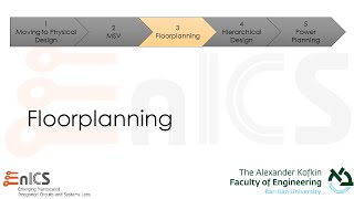
Floor Planning and Placement
Interactive Audio Lesson
Listen to a student-teacher conversation explaining the topic in a relatable way.
Introduction to Floor Planning
🔒 Unlock Audio Lesson
Sign up and enroll to listen to this audio lesson

Today we're going to discuss floor planning in VLSI design. Can anyone tell me what floor planning involves?

Is it about how we arrange the parts of a chip?
Exactly! Floor planning is about the arrangement of major functional blocks, ensuring efficient placement. What do you think is a key objective here?

Minimizing wirelength?
Great point! Minimizing wirelength helps reduce delays and power consumption. Remember the acronym MAP for: Minimize wirelength, Area Optimization, and Performance improvement. Can anyone explain why performance optimization is important?

It's about making sure everything talks to each other quickly!
Correct! This is crucial for meeting timing constraints. Let's summarize: Floor planning involves arranging functional blocks efficiently to minimize wirelength, optimize area, and improve performance.
Tools for Floor Planning
🔒 Unlock Audio Lesson
Sign up and enroll to listen to this audio lesson

Now let's talk about tools used in floor planning. Who can name a few tools that help in this process?

I've heard of Cadence Innovus!
Yes! Cadence Innovus is widely used in the industry for automation and optimization. How do you think these tools impact design efficiency?
They probably make the process faster and more accurate!
Right! They provide advanced algorithms for precise floor planning, reducing manual work. Remember, effective tools can significantly enhance productivity.
In summary, tools like Cadence Innovus and Synopsys IC Compiler II are essential for automating the floor planning process and improving design efficiency.
Placement Techniques
🔒 Unlock Audio Lesson
Sign up and enroll to listen to this audio lesson
Now let’s look at placement in VLSI design. What is the ultimate goal of the placement stage?
To minimize the delay and power consumption?
Exactly! Placement aims to strengthen timing and power efficiency. Who remembers the two types of placement?
Global and detailed placement!
Correct! Global placement is where we initially arrange cells, then detailed placement fine-tunes these positions. Can anyone explain what algorithms we might use for placement?
Simulated annealing and greedy algorithms?
Great! These algorithms help optimize the arrangement of cells to meet performance criteria. To recap: Placement minimizes delay and power while maximizing area efficiency using various techniques and algorithms.
Introduction & Overview
Read summaries of the section's main ideas at different levels of detail.
Quick Overview
Standard
Floor planning and placement are essential components of VLSI design that influence chip layout, power consumption, performance, and manufacturability. This section discusses the objectives, key factors, tools, and optimization strategies for effective floor planning and placement, ensuring efficient chip designs.
Detailed
Floor Planning and Placement
Floor planning and placement are pivotal stages in the physical design of Very-Large-Scale Integration (VLSI) chips. Understanding these processes is crucial, as they significantly affect performance, power consumption, area, and manufacturability of chips.
Key Points
- Definition and Importance: Floor planning sets the high-level arrangement of functional blocks, followed by placement, which optimizes the location of individual components within the plan.
- Objectives of Floor Planning: Key objectives include minimizing wirelength, optimizing area use, improving performance by strategically placing critical blocks, and ensuring adequate power distribution across the components.
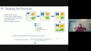
- Factors Affecting Floor Planning: Considerations such as block size and shape, connectivity, aspect ratio, and power distribution are critical for effective floor planning.
- Tools for Floor Planning: Industry-standard tools like Cadence Innovus and Synopsys IC Compiler II assist in automating and optimizing floor planning processes.
- Placement Strategies: Placement aims to minimize delay and power consumption while maximizing area efficiency through techniques like global and detailed placement approaches.
- Placement Algorithms: Common algorithms such as simulated annealing, force-directed methods, and greedy algorithms are employed to achieve optimal placement.
- Challenges: Despite advancements in tools, achieving optimal solutions poses challenges like managing design complexity, achieving timing closure, and ensuring manufacturability.
- Conclusion: Mastering floor planning and placement processes, along with the utilization of advanced techniques and tools, is crucial for producing efficient and manufacturable VLSI chip layouts.
Youtube Videos


Audio Book
Dive deep into the subject with an immersive audiobook experience.
Introduction to Floor Planning and Placement
Chapter 1 of 12
🔒 Unlock Audio Chapter
Sign up and enroll to access the full audio experience
Chapter Content
Floor planning and placement are critical stages in the physical design of VLSI chips, directly influencing the chip's performance, power consumption, area, and manufacturability. These steps ensure that the components (standard cells or blocks) of the design are arranged in such a way that the design can be implemented efficiently within the available area while meeting performance and power constraints. Floor planning refers to the initial stage of the physical design process where the high-level arrangement of functional blocks or cells is defined. Placement follows, where individual components are positioned within the predefined floor plan to optimize timing, area, and power consumption.
Detailed Explanation
In this chunk, we learn that floor planning and placement are fundamental processes in designing VLSI chips. Floor planning is the first step, where we arrange major components like processors and memory on the chip. Placement follows this by determining the exact position of smaller components to achieve the best timing, area efficiency, and power usage. Both steps are essential for ensuring the chip works effectively and fits well within its physical limits.
Examples & Analogies
Imagine designing a new restaurant. The floor plan represents how the dining area, kitchen, and restrooms are organized. Once the plan is done, you must decide where to place each table and chair to provide the best experience for customers and staff. Just like a restaurant’s layout impacts its operations, a chip’s floor plan affects its performance.
Objectives of Floor Planning
Chapter 2 of 12
🔒 Unlock Audio Chapter
Sign up and enroll to access the full audio experience
Chapter Content
The key goals of floor planning include:
● Minimizing Wirelength: By positioning blocks that are frequently connected near each other, floor planning minimizes the length of the interconnects, which reduces delay and power consumption.
● Area Optimization: Efficient placement of blocks ensures that the chip area is used optimally, avoiding wasted space and reducing the overall chip size.
● Performance Improvement: A good floor plan ensures that critical blocks are placed in positions that help meet timing constraints, reducing delay and increasing the chip’s overall speed.
● Power Distribution: Floor planning involves defining the layout for power distribution networks, ensuring that all blocks receive adequate power with minimal voltage drop.
Detailed Explanation
This chunk outlines the main objectives of floor planning for VLSI designs. One major goal is to minimize wirelength, which keeps the connections between components short, leading to lower delays and power needs. Another goal is area optimization, making sure that the chip uses space efficiently to avoid wasted areas, ultimately reducing size. Additionally, the arrangement helps improve overall performance by positioning critical components strategically to meet timing needs, and it ensures that power distribution throughout the chip is effective.
Examples & Analogies
Think of packing a suitcase for a trip. You want to place the items you use most often, like a toothbrush and shampoo, at the top for easy access. This minimizes the time needed to find them and optimizes space so everything fits well. In chip design, arranging components similarly ensures quick access to connections, reduces delays, and makes the most out of the available space.
Key Factors in Floor Planning
Chapter 3 of 12
🔒 Unlock Audio Chapter
Sign up and enroll to access the full audio experience
Chapter Content
● Block Size and Shape: The dimensions of each block should be carefully considered during floor planning. In general, blocks that are larger or more complex should be placed in locations that allow for optimal routing.
● Block Connections: Blocks that have high interaction (e.g., data transfer or communication) should be placed closer to each other to minimize wirelength and improve timing.
● Aspect Ratio: Maintaining an optimal aspect ratio for blocks helps minimize routing congestion and makes better use of available chip area.
● Power and Clock Distribution: Efficient power and clock grid design is essential for ensuring that the floor plan can support low-power operation and clock distribution with minimal skew.
Detailed Explanation
This chunk highlights important factors to consider during floor planning. Block size and shape are crucial; larger blocks need strategic placement to ease routing. Blocks that connect frequently should be located near one another to reduce wire length. The aspect ratio, or the proportions of blocks, should be optimal to prevent crowding and enhance space usage. Finally, ensuring a good design for power and clock distribution is vital for maintaining efficient operation and power management across the chip.
Examples & Analogies
Consider arranging furniture in a large room. Larger pieces, like sofas, should go against the walls to allow for easier movement around them. Chairs should be clustered around tables where people gather, reducing the distance for passing items back and forth. If everything is set up efficiently, it creates a functional and comfortable space. Similarly, in chip design, proper arrangements lead to better communication and performance.
Floor Planning Tools
Chapter 4 of 12
🔒 Unlock Audio Chapter
Sign up and enroll to access the full audio experience
Chapter Content
Several tools are available for floor planning that help designers automate and optimize the process:
● Cadence Innovus: A comprehensive tool used for floor planning, placement, and routing optimization. It integrates power, performance, and area considerations.
● Synopsys IC Compiler II: IC Compiler II offers an integrated approach for floor planning and optimization, providing features for both global and detailed floor planning.
● OpenROAD: An open-source tool for automated floor planning, placement, and routing, designed to handle large-scale designs efficiently.
Detailed Explanation
This chunk discusses tools that assist in the floor planning process for VLSI designs. Each tool, such as Cadence Innovus, Synopsys IC Compiler II, and OpenROAD, offers unique features that help designers automate tasks and optimize chip layouts. These tools streamline the design process by integrating various requirements like power and area considerations, ultimately improving the efficiency and effectiveness of floor planning.
Examples & Analogies
Think of using specialized software for organizing an event, like a wedding planner. They have tools to ensure the layout of tables, decorations, and guests flow smoothly and meet constraints like budget and space. Just as planners use tools to simplify their tasks, engineers use software to manage and optimize chip designs effectively.
Placement in VLSI Design
Chapter 5 of 12
🔒 Unlock Audio Chapter
Sign up and enroll to access the full audio experience
Chapter Content
Placement is the next step after floor planning, where individual cells or standard blocks are positioned within the floor plan. The objective of placement is to minimize delay, power consumption, and chip area while ensuring that the design meets its functional specifications.
Detailed Explanation
In this chunk, we learn about placement, which follows floor planning. Here, individual components or cells are precisely arranged within the defined floor plan. The focus during this phase is on minimizing delays, power use, and chip area while ensuring the design functions correctly. This step is crucial for maintaining the chip's operational parameters and efficiency.
Examples & Analogies
Picture a game of Tetris where each block represents a component of the chip. Just as you must fit the pieces together in a way that they don't overlap and fit within the play area, engineers also need to place their components accurately to avoid delays and ensure efficient space usage on the chip.
Objectives of Placement
Chapter 6 of 12
🔒 Unlock Audio Chapter
Sign up and enroll to access the full audio experience
Chapter Content
The main goals of placement include:
● Minimizing Delay: Ensuring that signals travel through the shortest possible path between cells, reducing signal propagation delay and improving the timing of the design.
● Reducing Power Consumption: Minimizing the length of power and signal interconnects can reduce both dynamic and static power consumption.
● Meeting Timing Constraints: Placement is crucial for ensuring that critical paths are optimized to meet the required setup and hold times.
● Maximizing Area Efficiency: Optimizing placement ensures that cells are positioned in such a way that the chip area is fully utilized while avoiding congestion and wasted space.
Detailed Explanation
This chunk outlines the main objectives of placement in VLSI design. The primary goal is to minimize delay by ensuring signals travel the shortest possible routes. This contributes to better overall timing for the design. Additionally, reducing the lengths of interconnects lowers power consumption, while making sure that critical paths meet timing requirements is crucial for the design's function. Lastly, optimizing placement helps maximize the use of chip area, preventing congestion and unnecessary waste.
Examples & Analogies
Think of a long assembly line where you want to minimize the time taken to move products from one station to another. If you arrange the stations so they are close to each other, the work can flow smoothly and quickly. In chip design, placement achieves a similar effect by ensuring signals move efficiently across the chip, addressing timing needs and power efficiency.
Placement Techniques
Chapter 7 of 12
🔒 Unlock Audio Chapter
Sign up and enroll to access the full audio experience
Chapter Content
Placement can be divided into global placement and detailed placement.
● Global Placement: Global placement involves an initial placement of cells across the entire chip. The goal is to minimize the total wirelength by positioning cells near their logical neighbors. During global placement, the designer does not worry about exact cell locations but focuses on reducing congestion and improving timing performance.
● Detailed Placement: Detailed placement is the refinement of the global placement. It fine-tunes the positions of cells to meet detailed constraints such as timing, signal integrity, and manufacturability. It involves adjusting the locations of cells to reduce routing congestion and satisfy design rules.
Detailed Explanation
This chunk introduces us to the two main types of placement: global and detailed. Global placement is the first broad stage, where cells are arranged in a way that reduces overall wire length without worrying about the exact positions. It’s about the bigger picture. Detailed placement follows, adjusting the positions more precisely to meet specific constraints, improving timing and manufacturability. This two-level approach ensures both broad efficiency and precise optimization in the final design.
Examples & Analogies
Imagine that you’re decorating a house. In the first phase, you might decide which rooms to put furniture in, focusing on flow and aesthetics—that's like global placement. In the second phase, you pick exactly where each piece of furniture goes, making sure everything fits well and looks good. This meticulous work is similar to the detailed placement process in chip design.
Placement Algorithms
Chapter 8 of 12
🔒 Unlock Audio Chapter
Sign up and enroll to access the full audio experience
Chapter Content
● Simulated Annealing: A probabilistic algorithm inspired by the annealing process in metallurgy. It iteratively adjusts the placement of cells to minimize wirelength and optimize for performance while avoiding local minima.
● Force-Directed Algorithms: These algorithms model the placement process as a system of forces, where cells are pushed and pulled to their optimal positions based on attractive and repulsive forces. The force-directed method can minimize wirelength and reduce congestion.
● Greedy Algorithms: Greedy algorithms place cells based on local optimization criteria. These algorithms are typically faster but may not achieve the global optimal placement.
Detailed Explanation
This chunk explains some common algorithms used in placement. Simulated annealing mimics a heating process, slowly adjusting cell placements to avoid settling at a less optimal solution. Force-directed algorithms treat placement as a physical process with forces acting on cells, resulting in refined positions that reduce wire length. Greedy algorithms focus on quick decisions based on immediate improvements, although they may miss globally better solutions in favor of faster results.
Examples & Analogies
Consider deciding on the best location for tents at a campsite. Using simulated annealing is like trying different configurations repeatedly to see what works best, taking time to adjust. The force-directed approach mimics how you might feel out the area, adjusting based on feedback from nature (like trees and rocks), while a greedy algorithm is like placing your tents wherever there’s flat ground without considering the overall layout. Each method has its strengths and weaknesses, similar to different strategies in placement algorithms.
Placement Tools
Chapter 9 of 12
🔒 Unlock Audio Chapter
Sign up and enroll to access the full audio experience
Chapter Content
● Cadence Innovus: Innovus offers an automated solution for placement, focusing on timing, power, and area optimization. It integrates both global and detailed placement strategies for optimal results.
● Synopsys IC Compiler II: Offers advanced placement capabilities, including timing optimization and power-aware placement for large-scale SoC designs.
● OpenROAD: An open-source tool that automates placement while balancing timing and area constraints, commonly used in academic research and smaller designs.
Detailed Explanation
This chunk presents several tools that help with the placement process in VLSI design. For example, Cadence Innovus automates placement while considering various factors like timing and power, making it efficient. Synopsys IC Compiler II provides robust features for more complex designs, ensuring that placement is optimized for speed and power usage. OpenROAD is an open-source option known for its ability to handle placement in smaller designs effectively. These tools streamline the placement task, allowing designers to focus on optimizing their layouts.
Examples & Analogies
Think of these tools like a GPS system when driving. Cadence Innovus provides turn-by-turn directions for your journey, ensuring you take the most efficient routes. Synopsys IC Compiler II is like a fancy system that also considers rush-hour traffic to optimize your time further. OpenROAD offers an accessible app for those who want straightforward routes without all the bells and whistles, helping you reach your destination quickly. In each case, the tools help simplify and enhance the process of reaching targeted outcomes in design.
Optimization Strategies for Performance and Area
Chapter 10 of 12
🔒 Unlock Audio Chapter
Sign up and enroll to access the full audio experience
Chapter Content
Both floor planning and placement have a significant impact on the final performance and area of the chip. Optimizing for performance and area often involves trade-offs.
● Performance Optimization: Critical Path Optimization: Ensuring that critical paths (paths that dictate the maximum clock speed) are placed with minimal delay.
● Retiming: Adjusting the placement of flip-flops in critical paths to balance delays and achieve timing closure.
● Area Optimization: Cell Resizing: Modifying the size of cells to optimize chip area while maintaining timing and power constraints.
● Block Merging: Combining smaller functional blocks into larger ones to save area and improve efficiency.
● Wirelength Minimization: By positioning related cells closer together, the overall wirelength is minimized, reducing both area and delay.
Detailed Explanation
This chunk explores strategies for optimization in both floor planning and placement. Performance optimization focuses on refining critical paths to reduce delays, as these paths determine how quickly the chip can operate. Retiming involves adjusting component placements to better manage delays, while area optimization includes resizing cells, merging blocks, and minimizing wire length. All these strategies work together to balance performance and area, which is crucial for efficient chip design.
Examples & Analogies
Imagine streamlining a delivery service. You want to ensure that the fastest routes are taken (like optimizing critical paths) while also ensuring that delivery vehicles are not overloaded (similar to resizing cells). Combining deliveries into larger shipments where possible saves trips and reduces overall costs, just as merging small blocks does within chip design. Both processes focus on improving efficiency while balancing multiple demands.
Challenges in Floor Planning and Placement
Chapter 11 of 12
🔒 Unlock Audio Chapter
Sign up and enroll to access the full audio experience
Chapter Content
Despite the advances in CAD tools, several challenges remain in achieving optimal floor planning and placement:
● Design Size: As SoCs grow in complexity, managing floor planning and placement becomes more difficult, requiring more advanced algorithms and computational power.
● Timing Closure: Achieving timing closure while optimizing for area and power is often a challenging task, especially in high-performance designs.
● Manufacturability: Ensuring that the floor plan and placement meet the manufacturing constraints (e.g., routing congestion, DRC violations) is a critical challenge.
Detailed Explanation
This chunk discusses the ongoing challenges in floor planning and placement despite technological advancements. One primary concern is the increasing complexity and size of system-on-chip (SoC) designs, which makes management more complicated and necessitates sophisticated algorithms. Another challenge is achieving timing closure, meaning all timing requirements are met while also optimizing for area and power, particularly under high-performance conditions. Lastly, manufacturability remains a critical issue, as the designed layout must adhere to specific manufacturing constraints to avoid problems during production.
Examples & Analogies
Think about organizing a large event, like a concert. The more performers and equipment, the harder it becomes to coordinate everything smoothly. You might need advanced systems to handle logistics and timing (just like sophisticated algorithms), while also ensuring that the venue has enough space and follows safety regulations. Similarly, in chip design, balancing complexity, timing, and manufacturability is crucial for successful outcomes.
Conclusion
Chapter 12 of 12
🔒 Unlock Audio Chapter
Sign up and enroll to access the full audio experience
Chapter Content
Floor planning and placement are critical steps in the physical design of VLSI chips. A well-optimized floor plan ensures that the design fits within the chip area, while placement ensures that timing, power, and area constraints are met. Advanced optimization techniques and tools, including simulated annealing, force-directed algorithms, and machine learning-driven placement, help achieve optimal performance and area. As VLSI designs continue to grow in size and complexity, these techniques and tools will remain essential for ensuring efficient, manufacturable chip layouts.
Detailed Explanation
The concluding chunk reiterates the significance of floor planning and placement in VLSI chip design. A properly optimized floor plan maximizes area usage, while effective placement aligns with timing, power, and area requirements. The adoption of advanced techniques and tools, such as machine learning and various algorithms, enhances the design process and helps meet the challenges posed by increasing complexity within designs. It assures that as technology progresses, these strategies will play a vital role in producing efficient and manufacturable chips.
Examples & Analogies
Think of a factory setup where the layout of machines and workstations determines how quickly a product can be manufactured. A well-structured factory layout (like a good floor plan) and strategic positioning of machines to optimize for speed and costs (similar to placement) ensure that production runs smoothly. Just as adaptive approaches are needed for factories, VLSI design requires effective planning and placement techniques to keep up with technological advancements.
Key Concepts
-
Floor Planning: The arrangement of functional blocks within a chip for optimal area and performance.
-
Placement: Positioning individual cells within the pre-defined floor plan to minimize delay.
-
Wirelength Minimization: The process of arranging components to reduce the interconnect length between them, aiding in performance.
-
Global vs. Detailed Placement: The two phases of placement, with global being initial and detailed being refinement.
Examples & Applications
Example of minimizing wirelength by placing frequently connected blocks closer together to reduce delay.
Using optimization tools like Cadence Innovus to automate the placement of cells efficiently.
Memory Aids
Interactive tools to help you remember key concepts
Rhymes
To plan the floor, blocks align, wire short and power fine.
Stories
Imagine a puzzle where every piece must fit perfectly; that’s how functional blocks must align in floor planning.
Memory Tools
Remember the acronym MAP for objectives: Minimize wirelength, optimize Area, and improve Performance.
Acronyms
For placement remember DAMP
Delay minimization
Area maximization
and Power reduction.
Flash Cards
Glossary
- Floor Planning
The process of arranging functional blocks within a chip's layout to optimize performance and area.
- Placement
The step that involves positioning individual cells within a predefined floor plan to reduce delay and optimize chip area.
- Wirelength Minimization
The objective of reducing the length of interconnects between components to improve performance and reduce power consumption.
- Global Placement
An initial phase of placement where cells are arranged across the entire chip without focusing on exact locations.
- Detailed Placement
The refinement of global placement, where cells' positions are adjusted to meet specific constraints.
- Optimization Techniques
Methods used to achieve better performance or area, such as critical path optimization and cell resizing.
Reference links
Supplementary resources to enhance your learning experience.