
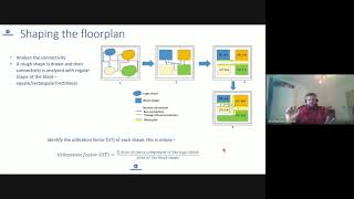
Objectives of Floor Planning
Interactive Audio Lesson
Listen to a student-teacher conversation explaining the topic in a relatable way.
Minimizing Wirelength
🔒 Unlock Audio Lesson
Sign up and enroll to listen to this audio lesson

Today, we're going to begin with one of the key objectives of floor planning: minimizing wirelength. Can anyone tell me why minimizing wirelength is so important in chip design?

I think it helps reduce delay in the signals, right?
Correct! Minimizing wirelength indeed helps reduce delay. Additionally, shorter wires help in lowering power consumption. Does anyone remember why that is?

Longer wires usually have more capacitance, which can drain more power.
Exactly! So, when we position blocks that communicate frequently near each other, we effectively accomplish two things: reducing delay and power use. Remember, we can use the acronym 'MWP' for Minimize Wirelength and Power!

That's a great way to remember it, MWP!
To summarize, minimizing wirelength is critical as it relates to both performance and power efficiency, forming the foundation of our floor planning discussions.
Area Optimization
🔒 Unlock Audio Lesson
Sign up and enroll to listen to this audio lesson

Now let's discuss area optimization—why is it vital for a chip’s design?

If we optimize the area, we can reduce the overall size of the chip, right?
That's correct! Optimizing the area ensures we use the space effectively and avoid wasted space. Does anyone have ideas on how this can also affect performance?
If we spend less area, we might have less delay due to shorter connections overall.
Perfect! By optimizing the arrangement of functional blocks, we can enhance both the chip’s footprint and its performance. Remember this with the phrase 'Efficient Area, Efficient Performance!'
Got it! Efficient Area leads to Efficient Performance.
Performance Improvement
🔒 Unlock Audio Lesson
Sign up and enroll to listen to this audio lesson
Next, we’ll delve into performance improvement. How do you think the placement of critical blocks matters?
Critical blocks need to be close to each other to meet timing constraints.
Absolutely! Proximity of critical blocks ensures faster signal propagation, thus enhancing overall speed. Can anyone tell me what can happen if these blocks are not optimally placed?
It could lead to delays and potentially slow down the whole chip's functioning.
Exactly! So, remember, the optimal placement of critical blocks is essential for performance. Use the mnemonic 'CLOSE for Critical Layout for Optimal Speed!'
That’s a useful way to remember it!
Power Distribution
🔒 Unlock Audio Lesson
Sign up and enroll to listen to this audio lesson
Finally, we address power distribution. What do you think is the role of power distribution networks in floor planning?
It’s important to ensure all blocks receive enough power without a significant voltage drop.
Exactly! An effectively designed power distribution network is vital for low power operation and performance. Does anyone recall what challenges can arise if power distribution is not optimized?
If the voltage drops too much, it could make parts of the circuit unreliable.
Correct, voltage drop can affect reliability. Remember, we should think of power distribution as the lifeline of the chip, which is why I like to say 'Power is Life!'
That's a catchy way to remember it!
Introduction & Overview
Read summaries of the section's main ideas at different levels of detail.
Quick Overview
Standard
Floor planning is a critical initial phase in chip design emphasizing essential objectives such as minimizing wirelength, optimizing area usage, improving performance, and ensuring effective power distribution. These objectives work together to enhance the overall efficiency and functionality of VLSI chips.
Detailed
Objectives of Floor Planning
Floor planning is a fundamental stage in VLSI design that significantly impacts the physical layout of a chip. The primary objectives include:
- Minimizing Wirelength: This objective aims to position blocks that frequently communicate close to each other to reduce the interconnect length, thereby minimizing delay and power consumption.
- Area Optimization: Effective arrangement ensures that the chip area is utilized efficiently, avoiding wasted space which contributes to a smaller overall chip size.
- Performance Improvement: Strategic placement of critical blocks is vital for meeting timing constraints and enhancing the chip's operational speed.
- Power Distribution: The layout should incorporate efficient power distribution networks to ensure all blocks receive adequate power with minimal voltage drop.
These objectives are critically intertwined, as optimizing wirelength, area, and performance while ensuring robust power distribution leads to a more efficient chip design that meets required specifications.
Youtube Videos


Audio Book
Dive deep into the subject with an immersive audiobook experience.
Minimizing Wirelength
Chapter 1 of 4
🔒 Unlock Audio Chapter
Sign up and enroll to access the full audio experience
Chapter Content
By positioning blocks that are frequently connected near each other, floor planning minimizes the length of the interconnects, which reduces delay and power consumption.
Detailed Explanation
Minimizing wirelength means arranging the various components or blocks of a chip as close together as possible if they need to communicate frequently. Imagine trying to connect two points with a string. The shorter the string, the less resistance there is in pulling it tight, which allows for faster communication and less energy use. In chip design, shorter connections (or interconnects) lead to faster signals and lower power consumption, which is crucial for efficient performance.
Examples & Analogies
Think of it like a group of friends who are all trying to communicate in a large room. If two friends (blocks) need to talk regularly, it's easier for them to stand next to each other rather than shouting across the room. This way, they can communicate quickly and with less effort.
Area Optimization
Chapter 2 of 4
🔒 Unlock Audio Chapter
Sign up and enroll to access the full audio experience
Chapter Content
Efficient placement of blocks ensures that the chip area is used optimally, avoiding wasted space and reducing the overall chip size.
Detailed Explanation
Area optimization is about efficiently using every part of the chip's surface. If you can pack the components tightly without overlapping, you end up with a smaller, more efficient design. This is similar to packing a suitcase: if you leave a lot of empty space, you can't fit in as many clothes or items. Therefore, strategically placing more blocks together signifies that designers need to consider the shapes and sizes of blocks carefully to maximize the limited space they have.
Examples & Analogies
Imagine you are packing for a trip. If you don’t fold your clothes properly and just toss them in, you’ll have a lot of wasted space in your suitcase. But when you roll or fold them strategically, you can fit more items inside without increasing the size of your suitcase. In floor planning, the goal is to fit more functional blocks within the existing chip area effectively.
Performance Improvement
Chapter 3 of 4
🔒 Unlock Audio Chapter
Sign up and enroll to access the full audio experience
Chapter Content
A good floor plan ensures that critical blocks are placed in positions that help meet timing constraints, reducing delay and increasing the chip’s overall speed.
Detailed Explanation
Performance improvement through floor planning focuses on ensuring that essential components of the chip are situated ideally to minimize delays in signals. For each chip, there are timing constraints that need to be adhered to for the device to operate efficiently. If critical operation blocks are placed far apart, it takes longer for signals to travel between them. Good planning helps align these blocks in such a way that data flows quickly across the chip, ultimately improving overall speed.
Examples & Analogies
Consider a busy highway system. If key routes to important destinations are planned in a way that minimizes travel time by placing major interchanges near each other, cars can move swiftly from point to point. Similarly, in a chip, if critical blocks are located close enough, the electronic signals can travel with minimal delay, boosting overall performance.
Power Distribution
Chapter 4 of 4
🔒 Unlock Audio Chapter
Sign up and enroll to access the full audio experience
Chapter Content
Floor planning involves defining the layout for power distribution networks, ensuring that all blocks receive adequate power with minimal voltage drop.
Detailed Explanation
Power distribution is essential in floor planning because every block on the chip needs reliable power to function properly. The layout must be designed to minimize any losses in power (voltage drop) as it travels through the wires to reach the components. Even a slight drop in voltage can cause some parts of the chip to underperform or act erratically. Therefore, a careful plan ensures that power flows efficiently, and effective routing minimizes losses.
Examples & Analogies
Think of water flowing through pipes to various parts of a house. If the pipes are too narrow or too long, water pressure reduces when it reaches the faucets, causing weak flow. If the plumbing is designed properly, water can reach all areas with good pressure, ensuring efficient use. In the same vein, the power distribution layout in floor planning helps maintain strong and balanced power supply to all chip blocks.
Key Concepts
-
Minimizing Wirelength: Reducing interconnect length to enhance speed and reduce power consumption.
-
Area Optimization: Efficiently using chip space to avoid waste and improve chip size.
-
Performance Improvement: Proper placement of functionally critical blocks to meet speed needs.
-
Power Distribution: Effective design ensuring reliable power supply with minimal voltage drop.
Examples & Applications
In a design where multiple blocks frequently communicate, placing them closely minimizes wirelength and optimizes performance.
Consider a chip where power distribution is poorly managed; voltage drops may occur, leading to instability in performance across various blocks.
Memory Aids
Interactive tools to help you remember key concepts
Rhymes
To make your chip run fine, keep wire paths snug and short, it's design's lifeline!
Stories
Imagine a town where shops are close together; they get more foot traffic. In chip design, keeping blocks close means faster communication and happier customers!
Memory Tools
Remember 'MAP': Minimize length, Area efficient, Performance boost!
Acronyms
Use 'WPAP' for Remembering Wirelength, Performance, Area, and Power.
Flash Cards
Glossary
- Wirelength
The total length of the interconnects between blocks in a chip design, influencing delay and power consumption.
- Area Optimization
The process of arranging chip blocks to use available space efficiently and minimize wasted area.
- Performance Improvement
Enhancements made in a chip design to ensure speed and meet timing constraints.
- Power Distribution
The method of delivering adequate power to all functional blocks in a chip layout to minimize voltage drop and ensure reliable operation.
Reference links
Supplementary resources to enhance your learning experience.