
Floor Planning in VLSI Design
Interactive Audio Lesson
Listen to a student-teacher conversation explaining the topic in a relatable way.
Introduction to Floor Planning
🔒 Unlock Audio Lesson
Sign up and enroll to listen to this audio lesson

Today, we start with floor planning in VLSI design, which is crucial for efficient chip layout. Can anyone tell me why floor planning is important?

Isn't it about organizing the components on the chip to use space efficiently?
Exactly! It's about arranging functional blocks like processors and memory to minimize wirelength and power consumption. This leads us to some key objectives of floor planning.

What are those key objectives?
Great question! They include minimizing wirelength, optimizing the area, improving performance, and ensuring effective power distribution.
Objectives of Floor Planning
🔒 Unlock Audio Lesson
Sign up and enroll to listen to this audio lesson

Let's break down these objectives. Minimizing wirelength helps reduce delay and power usage. Can someone explain how this might work?

By placing commonly connected blocks close together, right?
Spot on! This reduces the distance signals need to travel. Who can summarize the area optimization objective?

It's to ensure that the chip's physical area is used wisely, minimizing voids.
Exactly! Efficient block placement reduces overall chip size. Now, let's dive into the factors influencing these objectives.
Key Factors in Floor Planning
🔒 Unlock Audio Lesson
Sign up and enroll to listen to this audio lesson
When planning floors, block size and shape are critical considerations. Anyone wants to elaborate on this?
Larger blocks might need special placements for routing, right?
Exactly! And it's not just size; aspect ratio matters too, as it affects routing congestion. Can someone explain the role of block connections in floor planning?
Blocks that frequently communicate should be near to minimize wire length.
Well said! Lastly, who can tell me about the significance of power and clock distribution in floor planning?
It's to ensure all blocks get sufficient power without voltage drops!
Perfect! Now let's look at some tools that help automate these processes.
Floor Planning Tools
🔒 Unlock Audio Lesson
Sign up and enroll to listen to this audio lesson
Now, there are several tools for floor planning. Can someone name one?
Cadence Innovus?
Correct! Innovus helps with optimization considering power, performance, and area. Does anyone know another tool?
What about Synopsys IC Compiler II?
Absolutely! It's known for its integrated approach to floor planning. Lastly, anyone heard of an open-source tool?
OpenROAD, right?
Yes, well done! These tools greatly enhance our design process. Let's summarize what we've covered.
Introduction & Overview
Read summaries of the section's main ideas at different levels of detail.
Quick Overview
Standard
This section delves into floor planning in VLSI design, outlining its key objectives—such as minimizing wirelength and optimizing chip area—along with the critical factors that influence floor planning decisions, like block size, connections, and power distribution. Additionally, it highlights industry-standard tools used for these tasks.
Detailed
Floor Planning in VLSI Design
Floor planning is the initial step in defining a VLSI chip's physical layout, focusing on the arrangement of major functional blocks like processors and memory. Key objectives include minimizing wirelength, optimizing chip area, improving performance, and ensuring efficient power distribution. Critical factors in this process involve considering block size, shape, connections, and power distribution networks. Various tools, such as Cadence Innovus and Synopsys IC Compiler II, automate and enhance the floor planning task, leading to better chip designs that are efficient in terms of timing, power consumption, and area utilization.
Youtube Videos


Audio Book
Dive deep into the subject with an immersive audiobook experience.
Overview of Floor Planning
Chapter 1 of 4
🔒 Unlock Audio Chapter
Sign up and enroll to access the full audio experience
Chapter Content
Floor planning is the first step in defining the physical layout of a chip. It involves the global arrangement of major functional blocks (such as processors, memory, and I/O) on the chip to ensure that they are placed efficiently, with minimal wirelength and power consumption.
Detailed Explanation
Floor planning sets the foundation for how a chip will be physically arranged. By determining where major components like processors and memory will be located, designers can optimize the connections between these parts. This is crucial because shorter connections (or wirelengths) generally lead to lower energy consumption and better performance.
Examples & Analogies
Think of floor planning like organizing the layout of a grocery store. If the dairy section is far from the bakery, customers will have to walk more, which is inefficient. By placing related sections close together, customers can shop faster and more conveniently, similar to how a well-planned chip reduces delays in signal transmission.
Objectives of Floor Planning
Chapter 2 of 4
🔒 Unlock Audio Chapter
Sign up and enroll to access the full audio experience
Chapter Content
The key goals of floor planning include:
● Minimizing Wirelength: By positioning blocks that are frequently connected near each other, floor planning minimizes the length of the interconnects, which reduces delay and power consumption.
● Area Optimization: Efficient placement of blocks ensures that the chip area is used optimally, avoiding wasted space and reducing the overall chip size.
● Performance Improvement: A good floor plan ensures that critical blocks are placed in positions that help meet timing constraints, reducing delay and increasing the chip’s overall speed.
● Power Distribution: Floor planning involves defining the layout for power distribution networks, ensuring that all blocks receive adequate power with minimal voltage drop.
Detailed Explanation
These objectives highlight the importance of thinking carefully about the arrangement of different sections of the chip. Minimizing wirelength means designing connections that are as short as possible. Area optimization ensures the chip is compact, which is important for cost and performance. Performance improvement focuses on strategically placing the most 'important' blocks for speed, while power distribution emphasizes creating an efficient network to ensure that all parts of the chip operate reliably.
Examples & Analogies
It's like planning a city layout. If bus stops (important for transport) are placed too far from residential areas, people spend more time commuting (increasing delay). If commercial areas are compact and close to residential zones, it's easier for people to shop, promoting efficiency and reducing travel time (like wirelength). Proper infrastructure for power supply ensures that all areas can support the population effectively.
Key Factors in Floor Planning
Chapter 3 of 4
🔒 Unlock Audio Chapter
Sign up and enroll to access the full audio experience
Chapter Content
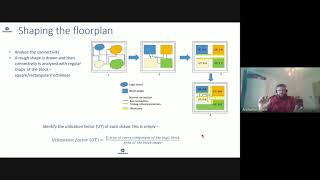
● Block Size and Shape: The dimensions of each block should be carefully considered during floor planning. In general, blocks that are larger or more complex should be placed in locations that allow for optimal routing.
● Block Connections: Blocks that have high interaction (e.g., data transfer or communication) should be placed closer to each other to minimize wirelength and improve timing.
● Aspect Ratio: Maintaining an optimal aspect ratio for blocks helps minimize routing congestion and makes better use of available chip area.
● Power and Clock Distribution: Efficient power and clock grid design is essential for ensuring that the floor plan can support low-power operation and clock distribution with minimal skew.
Detailed Explanation
This section emphasizes several important components that contribute to effective floor planning. The size and shape of blocks play crucial roles since larger components need to be placed in optimal spots to prevent routing problems. Additionally, the interactions between blocks dictate their proximity: blocks that frequently communicate should be close together to simplify wiring. Maintaining an optimal aspect ratio means adjusting the dimensions of blocks to avoid traffic jams in signal pathways, and having a solid plan for power supply is crucial for reliable performance without unwanted energy waste.
Examples & Analogies
Imagine a library. If the fiction section is huge, it should be in a larger room (considering size and shape). If people often borrow fiction and reference books together, those sections should be adjacent. A well-designed library layout makes it easy to access materials, just like a well-planned chip layout improves the flow of electrical signals.
Floor Planning Tools
Chapter 4 of 4
🔒 Unlock Audio Chapter
Sign up and enroll to access the full audio experience
Chapter Content
Several tools are available for floor planning that help designers automate and optimize the process:
● Cadence Innovus: A comprehensive tool used for floor planning, placement, and routing optimization. It integrates power, performance, and area considerations.
● Synopsys IC Compiler II: IC Compiler II offers an integrated approach for floor planning and optimization, providing features for both global and detailed floor planning.
● OpenROAD: An open-source tool for automated floor planning, placement, and routing, designed to handle large-scale designs efficiently.
Detailed Explanation
These tools incorporate advanced algorithms and functionalities to assist designers in creating efficient floor plans. Cadence Innovus combines various aspects of the design for a holistic approach, while Synopsys IC Compiler II helps with both an overview and finer details of planning. OpenROAD is particularly significant as an open-source platform that democratizes access to powerful floor planning solutions, making it possible for more users to engage with complex design challenges.
Examples & Analogies
Using these tools is like having sophisticated mapping software when planning a trip. Just as a map helps you find the best routes, avoid traffic, and ensure you have enough fuel, these tools allow engineers to navigate the complexities of chip design and optimize their plans to achieve the best outcomes.
Key Concepts
-
Minimizing Wirelength: Arrangement of blocks to reduce the length of interconnects, improving speed and power consumption.
-
Area Optimization: Efficient organization of the chip layout to maximize space utilization.
-
Power Distribution: Designing layouts for effective power delivery, enhancing chip performance.
Examples & Applications
Placing frequently communicating components such as a CPU and RAM close together to minimize wirelength.
Arranging logical blocks on the chip to avoid wasted space and improve layout efficiency.
Memory Aids
Interactive tools to help you remember key concepts
Rhymes
In the land of VLSI, blocks close by, minimize the wires, let power fly!
Stories
Imagine a busy city where the fire station (CPU) must be close to the hospitals (Memory) to save lives. In VLSI, keeping parts that talk to each other close saves time!
Memory Tools
ENGAGE: Efficiently Navigate Global Area for functionally aligned blocks and Efficient power routing.
Acronyms
W.A.P.P. – Wirelength, Area optimization, Performance, Power distribution.
Flash Cards
Glossary
- Wirelength
The total length of the interconnects between blocks on a chip, crucial for minimizing delay and power consumption.
- Area Optimization
The process of arranging blocks to make the best use of available chip area, effectively reducing waste.
- Power Distribution
The planned layout of power connections to ensure efficient power delivery across the chip.
- Aspect Ratio
The ratio of width to height of a block, which influences routing and space utilization.
- Floor Planning Tools
Software solutions that assist in the design and optimization of chip layout.
Reference links
Supplementary resources to enhance your learning experience.