
Conclusion
Interactive Audio Lesson
Listen to a student-teacher conversation explaining the topic in a relatable way.
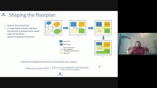
Importance of Floor Planning
🔒 Unlock Audio Lesson
Sign up and enroll to listen to this audio lesson

Today, we are discussing the critical role of floor planning in VLSI design. Can anyone tell me what you think floor planning is?

Isn’t it about arranging the major functional blocks on the chip?
Exactly! Floor planning involves the global arrangement of functional blocks. Why do you think minimizing wirelength and power consumption is important during this phase?

It helps in reducing delays and making the chip more efficient, right?
Correct! This can significantly improve the chip's performance. Remember the acronym WAP, which stands for Wirelength, Area, Performance because these are the core objectives of floor planning.

So, are there specific tools that help with this process?
Great question! Tools like Cadence Innovus and Synopsys IC Compiler II can help automate these tasks. Any questions on that?
Placement Techniques
🔒 Unlock Audio Lesson
Sign up and enroll to listen to this audio lesson

Now let’s talk about placement. Why do you think the placement of individual cells is crucial after floor planning?
It affects how signals travel between components, right?
Absolutely. Minimizing delay during placement ensures efficient signal propagation. Remember, the goal here is also to reduce power consumption. Let’s not forget about timing constraints! How might these constraints factor into placement?

We have to position critical paths correctly to meet setup and hold times.
Exactly! This is why both global and detailed placement are important. As a mnemonic, you can remember 'GD - Global first, Detail later'. Let's recap what we discussed today.
Optimization Techniques
🔒 Unlock Audio Lesson
Sign up and enroll to listen to this audio lesson
Today we're focusing on optimization techniques. Can anyone name one technique that can help with performance optimization during placement?
Critical path optimization?
Great answer! Critical path optimization is essential for ensuring minimal delay. Does anyone know another method?
Retiming can help, too, in balancing delays?
Exactly! Retiming adjusts the placement of flip-flops to achieve timing closure. Let’s not forget about area optimization. What strategies can be employed?
We can resize cells or merge blocks to save space.
Good suggestions! A good rule to remember is 'RMM - Resize, Merge, Minimize' for area optimization. Any final thoughts?
Challenges in VLSI Design
🔒 Unlock Audio Lesson
Sign up and enroll to listen to this audio lesson
What are some challenges that might arise in the floor planning and placement stages of VLSI design?
Complexity of designs can make management harder.
Exactly! As systems on chips grow, we face increased challenges in timing closure and manufacturability. Can anyone mention a constraint that can affect the layout?
Routing congestion could be a problem.
Correct! Ensuring that designs meet manufacturing constraints is crucial. Remember the acronym CMT - Complexity, Timing, Manufacturability. Let’s summarize what we’ve discussed.
Introduction & Overview
Read summaries of the section's main ideas at different levels of detail.
Quick Overview
Standard
The conclusion summarizes the critical role of floor planning and placement in VLSI design, noting that a well-optimized approach is necessary for achieving design goals related to performance, power consumption, and manufacturability. It highlights the significance of advanced optimization techniques and tools as designs become more complex.
Detailed
Conclusion
Floor planning and placement are critical steps in the physical design of VLSI chips. The effectiveness of these processes directly influences the chip's performance, power consumption, area utilized, and manufacturability. A well-optimized floor plan ensures that the design efficiently fits within the chip area, while the advanced placement of components ensures that all timing, power, and area constraints are met.
Advanced optimization techniques like simulated annealing and force-directed algorithms, alongside state-of-the-art tools, become indispensable as the complexity of VLSI designs increases. These methods not only address performance and area optimization but also adapt and evolve as technology advances. Consequently, the role of skilled designers who can navigate these modern challenges, utilizing sophisticated algorithms and tools, will remain vital in ensuring the successful realization of efficient and manufacturable chip layouts.
Youtube Videos


Audio Book
Dive deep into the subject with an immersive audiobook experience.
Importance of Floor Planning and Placement
Chapter 1 of 4
🔒 Unlock Audio Chapter
Sign up and enroll to access the full audio experience
Chapter Content
Floor planning and placement are critical steps in the physical design of VLSI chips.
Detailed Explanation
This chunk emphasizes that both floor planning and placement are essential processes in designing VLSI chips. Floor planning involves organizing the layout of the chip into functional blocks, while placement involves positioning individual components within those blocks.
Examples & Analogies
Think of designing a home. Floor planning is like deciding where the rooms (like the kitchen or living room) will be located, and placement is like figuring out where to position the furniture within those rooms.
Role of Optimization
Chapter 2 of 4
🔒 Unlock Audio Chapter
Sign up and enroll to access the full audio experience
Chapter Content
A well-optimized floor plan ensures that the design fits within the chip area, while placement ensures that timing, power, and area constraints are met.
Detailed Explanation
Optimization in both floor planning and placement is crucial because it helps maximize the efficiency of the design. A good floor plan uses chip space effectively, while placement ensures that all components can communicate quickly and efficiently without consuming too much power.
Examples & Analogies
Consider packing a suitcase for a trip. You want to fit as many items as possible (floor plan) while ensuring that you can easily access your clothes and avoid wrinkles (placement). Good packing saves space and keeps everything organized.
Advanced Techniques and Tools
Chapter 3 of 4
🔒 Unlock Audio Chapter
Sign up and enroll to access the full audio experience
Chapter Content
Advanced optimization techniques and tools, including simulated annealing, force-directed algorithms, and machine learning-driven placement, help achieve optimal performance and area.
Detailed Explanation
This chunk discusses the sophisticated methods and software utilized in floor planning and placement that help designers tackle the complex challenges of modern chip designs. Techniques such as simulated annealing and machine learning are used to find the best layouts that maximize performance while minimizing area and power consumption.
Examples & Analogies
Imagine you’re a chef trying to create a perfect dish. You need to experiment with different ingredients and cooking methods (advanced techniques) to find the best combination for a delightful meal. Similarly, engineers use various algorithms to iterate and improve chip designs.
Future of VLSI Design
Chapter 4 of 4
🔒 Unlock Audio Chapter
Sign up and enroll to access the full audio experience
Chapter Content
As VLSI designs continue to grow in size and complexity, these techniques and tools will remain essential for ensuring efficient, manufacturable chip layouts.
Detailed Explanation
The conclusion highlights that as technology advances, VLSI designs are becoming more intricate. This complexity necessitates the ongoing development and application of advanced design techniques and tools to ensure that chips can be manufactured effectively while still meeting necessary performance metrics.
Examples & Analogies
Think of building a large skyscraper. As architects work on bigger and more complex buildings, they rely on advanced software and methods to ensure structural integrity and functional design. The same goes for chip design engineers who utilize sophisticated tools to manage the growing complexity of VLSI projects.
Key Concepts
-
Floor Planning: The arrangement of major functional blocks on the chip.
-
Placement: Positioning of individual cells to optimize performance.
-
Optimization Techniques: Methods like simulated annealing and force-directed algorithms.
-
Timing Closure: The process of ensuring all timing constraints are satisfied.
-
Wirelength Minimization: The practice of reducing distances between connected components.
Examples & Applications
An example of effective floor planning is placing the processor close to memory blocks to reduce wirelength, enhancing speed.
Using simulated annealing in placement can lead to better optimization results compared to traditional methods.
Memory Aids
Interactive tools to help you remember key concepts
Rhymes
Plan it right, optimize in sight, makes the chip layout tight.
Stories
Imagine a city where roads are well planned. Short connections minimize traffic jams!
Memory Tools
Remember RMM for Area Optimization: Resize, Merge, Minimize!
Acronyms
Use WAP
Wirelength
Area
Performance for Floor Planning goals!
Flash Cards
Glossary
- Floor Planning
The initial stage of VLSI design that involves arranging functional blocks on a chip.
- Placement
The process of positioning individual cells or blocks in a predefined floor plan.
- Optimization
Techniques used to enhance chip performance regarding power consumption and area efficiency.
- Timing Closure
Achieving the required setup and hold times for signals in a circuit.
- Wirelength
The total length of interconnects on a chip, with implications for delay and power consumption.
Reference links
Supplementary resources to enhance your learning experience.