
Introduction to Floor Planning and Placement
Interactive Audio Lesson
Listen to a student-teacher conversation explaining the topic in a relatable way.
Understanding Floor Planning
🔒 Unlock Audio Lesson
Sign up and enroll to listen to this audio lesson

Today, we'll discuss floor planning, which is vital for efficient chip design. Can anyone explain what floor planning means?

Isn't it about arranging the components on the chip?
Exactly, Student_1! Floor planning involves the strategic placement of functional blocks to minimize wirelength and optimize area. Think of it as laying out a city where you want to keep schools, parks, and residential areas close together to reduce travel time — this reduces both delay and power consumption. A helpful acronym to remember is WAP — Wirelength, Area, Performance.

What role does power distribution play in floor planning?
Great question, Student_2! Power distribution ensures all blocks receive sufficient power with minimal voltage drop. So, an efficient layout can significantly affect how the chip performs!
To summarize, floor planning is about effectively arranging components to optimize wirelength, area, performance, and power distribution.
Placement Techniques in VLSI Design
🔒 Unlock Audio Lesson
Sign up and enroll to listen to this audio lesson

Now that we've covered floor planning, can anyone tell me what placement involves?

Is it about positioning the individual cells within the floor plan?
Correct, Student_3! Placement focuses on arranging individual cells to minimize delays and power consumption. Think of it like arranging furniture in a room to maximize space while keeping it easy to navigate.

What techniques do we use for placement?
Great inquiry, Student_4! There are several techniques like global placement, which finds an initial layout, and detailed placement, which fine-tunes that layout. Remember, the better the placement, the more efficient the chip. A common mnemonic here is ‘G-D’ for Global to Detailed.
In summary, placement is about positioning cells optimally to reduce delays and power usage while improving overall chip efficiency.
Optimization Strategies
🔒 Unlock Audio Lesson
Sign up and enroll to listen to this audio lesson
Let's talk about optimization strategies in floor planning and placement. Who can share some of the goals of these optimizations?
To minimize area and power consumption?
Exactly! Key goals include minimizing delay, reducing area usage, and optimizing power consumption. We also focus on timing constraints to ensure proper signal integrity and performance.
What tools can we use to help with optimization?
Exactly, Student_2! Tools like Cadence Innovus and Synopsys IC Compiler II assist in achieving efficient designs. They integrate various optimization techniques to streamline the process. Just remember, effective tool use can save us time while enhancing performance.
In summary, optimizing placement and floor planning is necessary to streamline chip design and ensure a functional, efficient layout.
Introduction & Overview
Read summaries of the section's main ideas at different levels of detail.
Quick Overview
Standard
This section provides an overview of floor planning and placement, emphasizing their importance in VLSI chip design. It highlights how these processes optimize the layout of circuits to meet performance and power constraints effectively.
Detailed
Introduction to Floor Planning and Placement
Floor planning and placement are critical phases in the physical design of VLSI (Very Large Scale Integration) chips, as they directly influence the chip's performance, power consumption, area, and manufacturability. Together, they ensure that the components (standard cells or blocks) of a design are organized effectively within the available area while adhering to performance and power constraints.
Key Points Covered in the Section
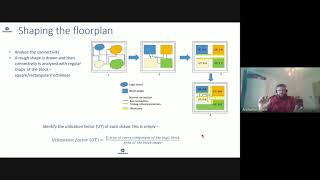
- Floor Planning: This is the preliminary stage where the high-level arrangement of functional blocks or cells is defined. It focuses on minimizing wirelength, optimizing area, improving performance, and ensuring proper power distribution.
- Placement: Following floor planning, this stage involves positioning individual components within the allotted space to further enhance timing, area utilization, and power efficiency.
- Optimization Techniques: Various methods and tools used in the industry aim to achieve optimal chip layouts through effective floor planning and placement.
Understanding these processes is essential for designers aiming to create efficient and manufacturable VLSI chips.
Youtube Videos


Audio Book
Dive deep into the subject with an immersive audiobook experience.
Importance of Floor Planning and Placement
Chapter 1 of 3
🔒 Unlock Audio Chapter
Sign up and enroll to access the full audio experience
Chapter Content
Floor planning and placement are critical stages in the physical design of VLSI chips, directly influencing the chip's performance, power consumption, area, and manufacturability. These steps ensure that the components (standard cells or blocks) of the design are arranged in such a way that the design can be implemented efficiently within the available area while meeting performance and power constraints.
Detailed Explanation
Floor planning and placement are essential to designing VLSI chips, which are used in most electronic devices today. They determine how well the chip works overall. By carefully arranging the components, engineers can ensure that the chip operates efficiently, consuming less power and taking up less space. If done poorly, it could lead to performance issues or even make the chip unmanufacturable.
Examples & Analogies
Think of floor planning like organizing a room. If you place all the furniture in a way that makes it hard to move around, using the room becomes inefficient. Conversely, if arranged smartly, you can navigate easily and use the space effectively. Similarly, good floor planning for a chip ensures that it functions optimally.
Understanding Floor Planning
Chapter 2 of 3
🔒 Unlock Audio Chapter
Sign up and enroll to access the full audio experience
Chapter Content
Floor planning refers to the initial stage of the physical design process where the high-level arrangement of functional blocks or cells is defined. Placement follows, where individual components are positioned within the predefined floor plan to optimize timing, area, and power consumption.
Detailed Explanation
Floor planning is the first step in designing a chip, creating a blueprint that lays out the main components without specifying their exact locations yet. After the floor plan is established, placement occurs, where specific cells are strategically placed within that layout to improve performance metrics like timing (how fast signals can travel), area (the space it uses), and power consumption (how much energy it wastes).
Examples & Analogies
Imagine building a house. First, you create a layout of where each room will be (this is floor planning). Next, you decide the exact location of the furniture within those rooms (this is placement). Just as good house design makes for a functional and comfortable living space, effective floor planning and placement make for a powerful and efficient chip.
Focus Areas in Floor Planning and Placement
Chapter 3 of 3
🔒 Unlock Audio Chapter
Sign up and enroll to access the full audio experience
Chapter Content
In this chapter, we discuss the process of floor planning, the principles behind placement optimization, and how these steps contribute to an efficient chip layout. We also explore various optimization techniques for performance and area and highlight the tools used in the industry for these tasks.
Detailed Explanation
The chapter outlines the process and importance of floor planning and placement in chip design. It emphasizes key strategies for optimizing chip layout concerning performance (how fast it operates), area (the physical size), and power consumption (energy usage). The discussion also includes tools that help engineers implement these strategies in a practical, efficient way.
Examples & Analogies
You can think of the optimization process like cooking a meal. First, you decide what dish you'll prepare (floor planning), then you gather and arrange your ingredients (placement), and finally, you might adjust the cooking times (optimization techniques) to enhance flavor and presentation. Culinary tools are like design software that helps you balance these components for the best final dish, which in this case, is a high-performing chip.
Key Concepts
-
Floor Planning: The arrangement of functional blocks on a chip to optimize space and performance.
-
Placement: Positioning of individual cells within the floor plan for efficient operation.
-
Wirelength Minimization: Reducing the total length of interconnections to improve speed and reduce power consumption.
-
Optimization: Techniques used to enhance chip layout performance and efficiency.
Examples & Applications
An example of floor planning is placing a processor, memory, and I/O sections close together to minimize wirelength.
In placement, arranging logic gates in a sequence that minimizes delay between operations is a practical application.
Memory Aids
Interactive tools to help you remember key concepts
Rhymes
To plan your floor, make it tight, Keep blocks close for power and speed — that's right!
Stories
Imagine a chef arranging ingredients on a counter; the closer they are, the faster and easier the cooking process.
Memory Tools
Remember 'WAP' for Floor Planning: W = Wirelength, A = Area, P = Performance.
Acronyms
F.O.P. for Floor Planning
= Functional Blocks
= Optimized Layout
= Power Distribution.
Flash Cards
Glossary
- Floor Planning
The initial stage of physical design where the arrangement of functional blocks is defined.
- Placement
The process of positioning individual components within a defined floor plan.
- Wirelength
The total length of interconnections in the chip layout, minimized to enhance performance.
- Power Distribution
The method of delivering power to all parts of the chip with minimal voltage drop.
- Optimization
The process of enhancing performance, area, or power consumption during design.
Reference links
Supplementary resources to enhance your learning experience.