
Key Factors in Floor Planning
Interactive Audio Lesson
Listen to a student-teacher conversation explaining the topic in a relatable way.
Block Size and Shape
🔒 Unlock Audio Lesson
Sign up and enroll to listen to this audio lesson

Let's discuss the importance of block size and shape in floor planning. Can anyone tell me why the size of functional blocks matters?

Maybe because larger blocks need more space around them?
Exactly! Larger or more complex blocks should be placed thoughtfully to optimize routing. This means putting them where they can connect efficiently. What is the consequence of not doing that?

It could increase delay and power consumption, right?
Yes! Remember the mnemonic 'Big Blocks Bear Better Routes' to help you recall that larger blocks should be positioned for optimal routing. Who can provide insights on the next key factor?
Block Connections
🔒 Unlock Audio Lesson
Sign up and enroll to listen to this audio lesson

Now, let’s move on to block connections. Why is it important to place blocks that frequently interact closer together?

Because it reduces wirelength, which can save power and improve performance?
Great answer! Maintaining proximity reduces delay. To remember this concept, think of 'Close The Circuit' – which emphasizes keeping connected blocks near each other. What other considerations play a role in our floor planning?

Aspect ratio is another key factor, isn’t it?
Aspect Ratio
🔒 Unlock Audio Lesson
Sign up and enroll to listen to this audio lesson
Correct! Let’s discuss aspect ratio. How does maintaining an optimal aspect ratio help us?
It helps to minimize routing congestion.
Absolutely! It also allows us to make better use of the available chip area. Remember to think 'Ratio for Routing' when you hear aspect ratio. Can anyone think of the last major factor in our floor planning discussions?
Power distribution!
Power and Clock Distribution
🔒 Unlock Audio Lesson
Sign up and enroll to listen to this audio lesson
Exactly! Efficient power and clock distribution are vital. What happens if the power grid isn’t designed well?
Blocks might not receive enough power, and voltage drops could occur.
Right! This leads to performance issues. Keep in mind to use 'Clock it Right!' when thinking about clock distribution to help remember its importance. Can we summarize what we’ve learned about the key factors in floor planning?
We covered block size and shape, block connections, aspect ratio, and the importance of power and clock distribution!
Introduction & Overview
Read summaries of the section's main ideas at different levels of detail.
Quick Overview
Standard
Key factors in floor planning include block size and shape, connections among blocks, aspect ratio, and power and clock distribution. Understanding these elements is essential for minimizing wirelength, optimizing area, and ensuring low power consumption in chip design.
Detailed
In VLSI design, effective floor planning directly impacts chip performance and manufacturability. Critical factors include:
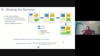
- Block Size and Shape: The layout of larger or complex blocks must optimize routing potential, ensuring they’re placed where they can achieve the best connections.
- Block Connections: Blocks that interact frequently should be nearby to reduce wirelength and enhance timing.
- Aspect Ratio: A well-maintained aspect ratio minimizes routing congestion, leading to better area utilization on the chip.
- Power and Clock Distribution: Efficient design of power and clock grids ensures optimal distribution for low power operation while minimizing skew. These factors collectively drive the goals of reducing power consumption, maximizing area, and improving performance.
Youtube Videos


Audio Book
Dive deep into the subject with an immersive audiobook experience.
Block Size and Shape
Chapter 1 of 4
🔒 Unlock Audio Chapter
Sign up and enroll to access the full audio experience
Chapter Content
● Block Size and Shape: The dimensions of each block should be carefully considered during floor planning. In general, blocks that are larger or more complex should be placed in locations that allow for optimal routing.
Detailed Explanation
When planning a floor layout for a chip, it's crucial to think about the size and shape of each block. Larger blocks or those that have complex functionalities need to be positioned thoughtfully. Placing them in strategic spots helps ensure that the pathways connecting these blocks are minimized. This optimal routing leads to better performance because it allows signals to travel shorter distances with less interference.
Examples & Analogies
Imagine packing a suitcase for a trip. If you have a large item, like a jacket, you want to place it in a specific spot where it can fit without crumpling or wasting space. Similarly, in chip design, large blocks need a suitable location to ensure that connections can be made easily and effectively.
Block Connections
Chapter 2 of 4
🔒 Unlock Audio Chapter
Sign up and enroll to access the full audio experience
Chapter Content
● Block Connections: Blocks that have high interaction (e.g., data transfer or communication) should be placed closer to each other to minimize wirelength and improve timing.
Detailed Explanation
In chip design, certain blocks interact more frequently than others, meaning they need to communicate or transfer data often. To make this communication faster and more efficient, these blocks should be positioned near each other. This proximity minimizes the length of the wires that connect them, which directly improves performance by reducing the time it takes for signals to travel between blocks.
Examples & Analogies
Think of a group of friends at a party who want to chat. If they're all spread out across the room, they'll have to shout to be heard, which takes longer. But if they stand close together, their conversations can flow easily and quickly. In the same way, placing communicating blocks close together enhances the efficiency of data exchange in the chip design.
Aspect Ratio
Chapter 3 of 4
🔒 Unlock Audio Chapter
Sign up and enroll to access the full audio experience
Chapter Content
● Aspect Ratio: Maintaining an optimal aspect ratio for blocks helps minimize routing congestion and makes better use of available chip area.
Detailed Explanation
The aspect ratio refers to the relationship between the width and height of a block. Properly maintaining this ratio is essential for making efficient use of space on the chip. A well-proportioned block reduces congestion when routing wires because it helps in managing how signals are distributed across the chip, leading to improved overall performance and area usage.
Examples & Analogies
Consider designing a rectangular garden. If the width and length are well-balanced, it's easier to plant flowers and maintain the space. However, if one side is too long or short, it can complicate planting and access. Similarly, in chip design, maintaining a balanced aspect ratio helps streamline routing and makes the layout more efficient.
Power and Clock Distribution
Chapter 4 of 4
🔒 Unlock Audio Chapter
Sign up and enroll to access the full audio experience
Chapter Content
● Power and Clock Distribution: Efficient power and clock grid design is essential for ensuring that the floor plan can support low-power operation and clock distribution with minimal skew.
Detailed Explanation
In chip design, providing power and clock signals evenly across the layout is critical. A well-designed grid ensures that every part of the chip receives adequate power without significant drops in voltage. Additionally, careful clock distribution minimizes timing discrepancies (skew). Having a uniform power supply and synchronized clock signals enhances performance and reliability.
Examples & Analogies
Think of a concert where the sound system is set up to ensure every part of the audience hears the music at the same volume and tempo. If some areas get louder or are out of sync, it detracts from the performance. Similarly, in a chip, efficient power and clock distribution ensures each section operates optimally and in harmony with the others.
Key Concepts
-
Block Size and Shape: Consider the dimensions of blocks to optimize routing and design efficiency.
-
Block Connections: Place interacting blocks closer to each other to minimize delay and power consumption.
-
Aspect Ratio: Ensure a favorable width-height ratio for blocks to reduce congestion.
-
Power Distribution: Design adequate power distribution networks to minimize voltage drop and support performance.
Examples & Applications
When designing a chip that includes a processing unit and memory, placing these blocks in close proximity reduces the wirelength needed for data transfer.
If a chip's functional blocks are not positioned optimally, it could lead to excessive wirelength, which may hinder performance and increase power consumption.
Memory Aids
Interactive tools to help you remember key concepts
Rhymes
Big Blocks Bear Better Routes, when they’re placed without any doubts.
Stories
Imagine a city where all main roads lead to central blocks; the shorter the road, the faster goods travel, reflecting how interconnected blocks should be laid out.
Memory Tools
Remember 'Close The Circuit' for placing connected blocks near each other.
Acronyms
P-A-C for Power, Aspect ratio and Connections fundamental to floor planning.
Flash Cards
Glossary
- Floor Planning
The initial stage in VLSI design where the arrangement of functional blocks is defined.
- Block Size and Shape
The dimensions and configuration of functional blocks in a chip design impacting routing and performance.
- Block Connections
The relationships between functional blocks that need to communicate, impacting their placement relative to each other.
- Aspect Ratio
The proportional relationship between width and height of a block, affecting layout efficiency.
- Power Distribution
The chemical pathway designed to distribute electrical power across different blocks on the chip.
- Clock Distribution
The method of distributing the clock signal among various components within the chip to ensure synchronization.
Reference links
Supplementary resources to enhance your learning experience.