
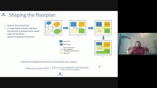
Challenges in Floor Planning and Placement
Interactive Audio Lesson
Listen to a student-teacher conversation explaining the topic in a relatable way.
Design Size Challenges
🔒 Unlock Audio Lesson
Sign up and enroll to listen to this audio lesson

Today, we're going to discuss the challenge of increasing design sizes in floor planning and placement. As chips become more complex, what do you think is one of the main issues we face?

I think managing the different components must be harder with larger designs.
Spot on! Larger designs require advanced algorithms and more computational power. Could someone give me an example of how this might impact the layout?

Maybe it leads to increased routing congestion or longer wire lengths?
Exactly! More complexity typically translates to greater challenges in optimizing wire lengths and reducing congestion.

How do designers manage these increased complexities?
They utilize advanced algorithms and enhanced computational techniques to better handle the increased design sizes.
Let's summarize: larger designs lead to more complexities requiring advanced algorithms and computational resources.
Timing Closure
🔒 Unlock Audio Lesson
Sign up and enroll to listen to this audio lesson

Let's move on to timing closure. Can someone tell me what this means in the context of VLSI design?

It's about ensuring that all timing requirements are met, right?
Correct! It's crucial, especially in high-performance designs. Why might achieving timing closure conflict with other goals?
Because you might have to prioritize timing over area or power optimization?
Precisely! There's often a trade-off between these factors. Does anyone remember a technique used to help achieve timing closure?
I think retiming is one method.
Exactly! Retiming moves flip-flops and can help balance delays effectively.
In summary, timing closure is about meeting critical timing requirements, which can conflict with area and power optimizations.
Manufacturability Challenges
🔒 Unlock Audio Lesson
Sign up and enroll to listen to this audio lesson
Next, let's discuss manufacturability. Why is this an important challenge in floor planning and placement?
It affects how well a chip can be produced in factories.
Exactly! If the design doesn't adhere to manufacturing constraints like routing congestion, it can lead to production issues.
What kind of issues can arise from DRC violations?
Great question! DRC violations can lead to defective chips, which impacts yield and performance.
So, ensuring that the floor plan is manufacturable is critical?
Yes! Ensuring manufacturability directly influences the reliability and cost-effectiveness of the final product.
Let's wrap up: manufacturability is key to ensuring production efficiency and chip reliability.
Introduction & Overview
Read summaries of the section's main ideas at different levels of detail.
Quick Overview
Standard
The section outlines several key challenges including design size, timing closure, and manufacturability that complicate the process of achieving optimal floor planning and placement in VLSI chips. It emphasizes the need for advanced algorithms and tools to address these issues.
Detailed
Challenges in Floor Planning and Placement
Despite significant advancements in Computer-Aided Design (CAD) tools for VLSI design, several challenges remain in achieving optimal floor planning and placement. These challenges are crucial as they impact the efficiency and functionality of integrated circuits...
Key Challenges:
- Design Size: As System on Chips (SoCs) grow in complexity, the floor planning and placement become increasingly intricate, necessitating advanced algorithms and greater computational power to manage these designs.
- Timing Closure: Ensuring that all timing requirements are met while simultaneously optimizing for power and area is a persistent challenge, especially in high-performance designs where timing constraints are stringent.
- Manufacturability: The floor plan and placement must adhere to manufacturing constraints, including avoiding routing congestion and ensuring Compliance with Design Rule Check (DRC) violations, which directly affects yield and performance.
By understanding these challenges, designers can leverage advanced tools and techniques to better navigate the complexities of VLSI design.
Youtube Videos


Audio Book
Dive deep into the subject with an immersive audiobook experience.
Design Size
Chapter 1 of 3
🔒 Unlock Audio Chapter
Sign up and enroll to access the full audio experience
Chapter Content
As SoCs grow in complexity, managing floor planning and placement becomes more difficult, requiring more advanced algorithms and computational power.
Detailed Explanation
This chunk highlights the challenge of increasing complexity in System on Chips (SoCs). As technology advances, designs become more intricate, with numerous components that need to be arranged within a chip. This complexity makes it hard for designers to make efficient floor plans and placements, which in turn leads to the necessity of sophisticated algorithms and significant computational resources to manage this complexity effectively.
Examples & Analogies
You can think of managing the floor plan of an SoC like organizing a huge music festival. Initially, it might be straightforward to arrange a few performers on a small stage, but as more bands join and the festival grows, ensuring that each performer has enough space and the right connections to power and sound equipment becomes substantially more challenging.
Timing Closure
Chapter 2 of 3
🔒 Unlock Audio Chapter
Sign up and enroll to access the full audio experience
Chapter Content
Achieving timing closure while optimizing for area and power is often a challenging task, especially in high-performance designs.
Detailed Explanation
Timing closure refers to the process of adjusting the design so that all timing constraints are met. This means that signals must arrive at their destinations in the appropriate timeframe for the chip to function correctly. Balancing this requirement with the goals of minimizing area (the physical space the chip occupies) and power consumption (how much energy it uses) can be difficult. Designers must continually tweak the design and placement until they have satisfied all these constraints, which often requires careful planning and iteration.
Examples & Analogies
Imagine trying to bake a cake that is both fluffy and large enough to serve a crowd, while also making sure it has the right flavor. Each time you adjust one element—like reducing sugar to cut calories or increasing egg whites for fluffiness—it might affect how the cake bakes and rises. Similarly, in chip design, adjustments can impact timing and performance, making it vital to achieve a perfect balance.
Manufacturability
Chapter 3 of 3
🔒 Unlock Audio Chapter
Sign up and enroll to access the full audio experience
Chapter Content
Ensuring that the floor plan and placement meet the manufacturing constraints (e.g., routing congestion, DRC violations) is a critical challenge.
Detailed Explanation
Manufacturability involves making sure that the design can actually be produced in a factory without issues. This includes adhering to various constraints like Design Rule Checking (DRC), ensuring that wires do not cross too closely, and avoiding routing congestion where too many connections might cause problems during fabrication. If a design fails to meet these manufacturing constraints, it can lead to defects or even total product failure. Therefore, achieving a design that is both functional and manufacturable is a significant challenge for engineers.
Examples & Analogies
Think of manufacturability like constructing a highway system. If the roads (wires) are too close together or poorly designed, traffic jams and accidents can occur (routing congestion). Just as engineers must follow strict rules when designing a highway—such as proper spacing between roads to ensure vehicles can navigate safely—chip designers must follow manufacturing guidelines to ensure that chips can be produced without defects.
Key Concepts
-
Design Size: Refers to the overall complexity of a design and how it impacts floor planning and placement.
-
Timing Closure: A critical process in VLSI design that ensures all timing requirements are met, impacting overall design performance.
-
Manufacturability: The extent to which a design can be produced effectively, avoiding DRC violations and routing congestion.
Examples & Applications
As chips increase in design size, the interaction between components leads to routing congestion, necessitating more sophisticated planning algorithms.
When timing closure isn't met, a design might fail to function as intended, illustrating the balance between performance and manufacturability.
Memory Aids
Interactive tools to help you remember key concepts
Rhymes
With design size on the rise, timings must finalize, or routing's demise.
Stories
In a town where technology thrived, the chipmakers faced the giant of design size. With every chip, they battled to close the timings and keep the factories running smoothly under the constraints of manufacturability.
Memory Tools
Remember 'DMT' – Design size, Manufacturability, Timing closure for three key challenges.
Acronyms
For DCM – Design Complexity Management
Critical for success in VLSI challenges.
Flash Cards
Glossary
- Design Size
The overall complexity and the number of components within a VLSI chip, affecting planning and placement.
- Timing Closure
The process of ensuring that all timing constraints for signals in a VLSI design are met.
- Manufacturability
The ability to produce a chip efficiently while avoiding errors in the design that affect production.
Reference links
Supplementary resources to enhance your learning experience.