
Key DFM Techniques
Interactive Audio Lesson
Listen to a student-teacher conversation explaining the topic in a relatable way.
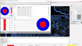
Design Rule Checking (DRC)
🔒 Unlock Audio Lesson
Sign up and enroll to listen to this audio lesson

Today, we're going to discuss Design Rule Checking, or DRC. Can anyone tell me what DRC is and why it's important?

Isn't DRC about making sure the design adheres to specific rules for spacing and features?
Exactly, Student_1! DRC ensures that the chip design does not violate manufacturing requirements. It helps prevent defects that could occur during fabrication. Remember the acronym DRC? It stands for 'Design Rule Checking.'

What happens if there are DRC violations?
Good question, Student_2! DRC violations can lead to defects in the final product. The aim of DFM is to identify these violations early so they can be fixed before manufacturing. DRC helps improve yield!

How do we actually check for those violations?
DRC is checked using EDA tools like Cadence Allegro or Mentor Graphics Calibre. They automatically verify the design against predefined rules. Remember, a well-checked layout is key to successful manufacturing!

So, it's really about preventing problems before they happen!
Exactly! To summarize, DRC is crucial for ensuring designs are manufacturable and reduces the risk of defects during production.
Minimizing Process Variations
🔒 Unlock Audio Lesson
Sign up and enroll to listen to this audio lesson

Now, let’s discuss minimizing process variations. What do we mean by that, anyone?
I think it’s about reducing differences in manufacturing that can affect how a chip works, right?
That's correct, Student_1! Minimizing process variations means designing circuits that perform consistently despite changes in manufacturing conditions. This approach increases yield.
How do we design circuits that are less sensitive to these variations?
Great follow-up, Student_2. It involves adjusting design margins and optimizing layout geometries to ensure robustness. Think of it as making designs less ‘finicky’ during production!
So if we do this, we can avoid surprises later on?
Exactly, Student_3! By accounting for potential variances in the manufacturing process, DFM helps to create reliable chips. Ensure you remember that minimizing variations is crucial for quality. Let’s recap: Reducing process variations improves yield and chip performance.
Minimizing Interconnect Length
🔒 Unlock Audio Lesson
Sign up and enroll to listen to this audio lesson
Now, let's talk about minimizing interconnect length. Why do you think this is important?
Maybe because longer interconnects could slow down signals?
You're on the right track, Student_1! Longer interconnects result in increased delays, power consumption, and can even affect signal integrity. That's why DFM encourages optimizing the routing to keep interconnects as short as possible.
How can we achieve that?
Using compact layouts and efficient routing strategies helps. Think of it as taking the most direct route to your destination to save time and energy! What else do shorter interconnects help with, Student_3?
They probably make the whole chip more reliable too!
Exactly! Minimized interconnect lengths lead to a more manufacturable and reliable design. In summary, short interconnects are better for performance, reliability, and manufacturability.
Cell and Layout Optimization
🔒 Unlock Audio Lesson
Sign up and enroll to listen to this audio lesson
Let’s discuss cell and layout optimization. What advantages do standardized cells offer?
I think they help fit within the manufacturing constraints easily.
Right, Student_1! Standardized cells reduce defects by ensuring compatibility with manufacturing processes. This optimization can significantly enhance yield.
But how do we optimize the layout?
Good question, Student_2! Optimizing layout involves carefully placing cells to minimize distances and avoid congestion, which helps ensure efficient paths for signal propagation.
So, it’s about designing for efficiency?
Exactly! Efficient design leads to fewer defects during production. To summarize, using standardized cells and optimizing their layout enhances manufacturability and yield.
Via Optimization and Hotspot Analysis
🔒 Unlock Audio Lesson
Sign up and enroll to listen to this audio lesson
Finally, let’s dive into via optimization and hotspot analysis. What is the role of vias in circuit design?
Vias connect different metal layers, right?
Correct, Student_1! However, excessive vias can introduce resistance and capacitance, impacting performance negatively. DFM aims to minimize via usage through optimized layouts.
How do we know where to focus on hotspots in the layout?
Hotspot analysis tools identify areas where heat or electrical stress could lead to reliability issues. Designers can optimize these regions to enhance performance and longevity.
So it’s about both minimizing vias and addressing problem areas?
Exactly, Student_3! By optimizing vias and being proactive about hotspots, we can create a chip that is not only manufacturable but also reliable. To wrap up, always remember that both are key aspects of DFM.
Introduction & Overview
Read summaries of the section's main ideas at different levels of detail.
Quick Overview
Standard
Key DFM techniques such as Design Rule Checking (DRC), Minimizing Process Variations, and Optimizing Layout and Interconnects are discussed to illustrate how these methods contribute to reducing defects, improving chip yield, and ensuring overall manufacturability during the production process.
Detailed
Detailed Summary
This section focuses on the Key DFM Techniques which are crucial for ensuring that the designs of chips are manufacturable with minimal defects. The following techniques are emphasized:
- Design Rule Checking (DRC): Ensures that the layout adheres to the minimum spacing and feature size requirements defined by the manufacturing process. Violations can lead to production defects, making DRC a critical area of focus.
- Minimizing Process Variations: In this context, DFM aims to design circuits that are robust against variations in manufacturing processes. By adjusting design margins and layout geometries, defects due to process variations can be mitigated.
- Minimizing Interconnect Length: Long interconnects can cause significant delays and power consumption issues. DFM advocates for compact routing strategies to enhance reliability and performance.
- Via Optimization: The use of vias in VLSI designs can introduce resistance and capacitance that degrade performance. DFM strategies focus on limiting excessive via utilization through careful layout planning.
- Cell and Layout Optimization: Utilizing standardized, compact cells ensures compatibility with manufacturing constraints. Optimized placement of these cells is also essential for minimizing defects.
- Hotspot Analysis: Identify and optimize areas in the layout that could lead to high current and reliability issues. Addressing these hotspots prevents potential failures in the manufactured product.
Through these techniques, DFM helps to enhance product yield, reduce manufacturing costs, and improve time-to-market by ensuring designs are optimized for the realities of chip production.
Youtube Videos


Audio Book
Dive deep into the subject with an immersive audiobook experience.
Design Rule Checking (DRC)
Chapter 1 of 6
🔒 Unlock Audio Chapter
Sign up and enroll to access the full audio experience
Chapter Content
DRC ensures that the design meets the minimum feature sizes and spacing requirements for the manufacturing process. DRC violations can lead to defects during fabrication, and DFM aims to reduce or eliminate such violations.
Detailed Explanation
Design Rule Checking (DRC) is a critical step in the design for manufacturability process. It verifies whether the design adheres to certain established rules regarding minimum sizes and spacing for the components. If the design violates any of these rules, it can cause problems during manufacturing, such as creating defects that may affect chip performance. DFM focuses on reducing these violations to ensure a smoother manufacturing process.
Examples & Analogies
Imagine you’re baking a cake. If you don’t follow the recipe's measurements and spacing, the cake can fall apart or not cook properly. Similarly, DRC ensures that 'ingredients' in the chip design are placed correctly and at the right sizes to avoid a 'defective cake' during manufacturing.
Minimizing Process Variations
Chapter 2 of 6
🔒 Unlock Audio Chapter
Sign up and enroll to access the full audio experience
Chapter Content
DFM involves designing circuits that are less sensitive to variations in the manufacturing process, such as variations in transistor sizes, line widths, and doping levels. This can involve adjusting design margins and optimizing layout geometry to account for these variations.
Detailed Explanation
Minimizing process variations is essential for ensuring that the chips function reliably across different manufacturing conditions. Variations can occur due to differences in transistor sizes, line widths, and material properties. DFM techniques aim to create designs that can tolerate these variations by carefully adjusting design parameters and layout shapes. This way, even if there are small manufacturing differences, the functionality of the chips remains intact.
Examples & Analogies
Think of it like tailoring a suit. If a suit is cut too close to the exact measurements, even a slight weight gain or loss can make it fit poorly. However, if the tailor allows for minor adjustments, the suit remains comfortable regardless of minor changes. Similarly, designs that can accommodate variations will perform better in production.
Minimizing Interconnect Length
Chapter 3 of 6
🔒 Unlock Audio Chapter
Sign up and enroll to access the full audio experience
Chapter Content
DFM seeks to reduce the length of interconnects, as longer interconnects are more prone to delays, signal degradation, and power consumption. By optimizing the routing of interconnects, the design is made more manufacturable and reliable.
Detailed Explanation
Interconnects are the pathways that connect different parts of a chip. Longer interconnects can lead to delays in signal transmission, degrade signal quality, and increase power consumption. DFM advocates for minimizing these lengths to improve the overall performance and reliability of the chip. By optimizing how interconnects are routed in the design, manufacturers can enhance the manufacturability of the chip.
Examples & Analogies
Consider a series of roads connecting multiple destinations. If one road is very long and poorly maintained, it might take longer to travel between points. By creating shorter, well-maintained routes, travelers can reach their destinations quicker and with less hassle. Likewise, minimizing interconnect length helps chips operate more efficiently.
Via Optimization
Chapter 4 of 6
🔒 Unlock Audio Chapter
Sign up and enroll to access the full audio experience
Chapter Content
In VLSI designs, vias are used to connect different metal layers. Excessive via usage can increase the resistance and capacitance of interconnects, leading to power loss and performance degradation. DFM aims to minimize via usage by optimizing the layout.
Detailed Explanation
Vias are critical components in VLSI designs, enabling connections between layers of metal in a chip. However, overusing vias can introduce problems like increased resistance and capacitance, which can lead to power loss and slower performance. DFM strategies focus on optimizing via usage, ensuring that the layout makes efficient use of vias, thereby preserving signal integrity and reducing unwanted power losses.
Examples & Analogies
Imagine a multi-level parking garage. If too many ramps are used to connect levels, it might slow down traffic flow and make navigation difficult. Optimizing the number of ramps helps keep traffic smooth and efficient. Similarly, reducing unnecessary vias in chip design keeps electronic signals flowing efficiently.
Cell and Layout Optimization
Chapter 5 of 6
🔒 Unlock Audio Chapter
Sign up and enroll to access the full audio experience
Chapter Content
Using compact, standardized cells in the design and optimizing their placement can reduce the number of defects and ensure that the chip is easier to manufacture. Standardized cells also help in making sure that they fit within the manufacturing process constraints.
Detailed Explanation
Cell and layout optimization focuses on utilizing standardized design cells, which are pre-designed functional blocks that can simplify the design process. By employing these standardized cells and optimizing their placement, the designer can minimize defects and streamline manufacturing. This also helps to ensure that the design complies with various manufacturing constraints, improving overall yield.
Examples & Analogies
Think about using pre-made furniture instead of custom-built pieces for every room in a house. Standardized furniture fits well in common spaces and simplifies the process. Similarly, standardized cells streamline chip design and help ensure smooth manufacturing.
Hotspot Analysis
Chapter 6 of 6
🔒 Unlock Audio Chapter
Sign up and enroll to access the full audio experience
Chapter Content
DFM tools analyze potential 'hotspots' in the layout—areas where high current, heat, or power may cause reliability issues. By optimizing these regions, designers can prevent reliability issues in the final product.
Detailed Explanation
Hotspot analysis identifies areas in a chip layout that could overheat or experience high current levels, leading to potential failure. By using specialized DFM tools to analyze these areas, designers can make necessary adjustments to ensure that these hotspots do not compromise the chip’s reliability. The aim is to maintain performance and avoid malfunctions during the chip's operation.
Examples & Analogies
Consider a city's power grid. If certain areas draw too much power, they may become overloaded and fail. By monitoring and optimizing these 'hotspots', city planners can ensure reliable electricity supply. Similarly, hotspot analysis in chip design ensures that critical areas are managed to prevent issues.
Key Concepts
-
Design Rule Checking (DRC): Ensures adherence to manufacturing specifications to prevent defects.
-
Minimizing Process Variations: Designs circuits robust to manufacturing inconsistencies.
-
Minimizing Interconnect Length: Shorter connections improve performance and reliability.
-
Via Optimization: Reduces the negative impact of excessive vias on performance.
-
Cell and Layout Optimization: Standardized cells improve manufacturability.
-
Hotspot Analysis: Identifies areas for performance and reliability improvements.
Examples & Applications
A chip design that undergoes extensive DRC ensures higher yield by preventing defects related to incorrect spacing.
By optimizing interconnect layouts, designers can enhance signal integrity, leading to faster and more reliable performance.
Memory Aids
Interactive tools to help you remember key concepts
Rhymes
DRC's the key, to check the rules, keeps designs neat, avoiding tools' drools!
Stories
Imagine a chef (the layout designer) ensuring all ingredients (design rules) are perfectly measured to create a flawless dish (the chip). Ignoring this leads to burning or undercooked areas (defects) in the final meal!
Memory Tools
To remember the DFM techniques, think 'DRIM CoH': DRC, Reduce Variations, Interconnect Length, Minimize Vias, Cell Optimization, Hotspot Analysis.
Acronyms
Remember DFM as 'Design for Fabulous Manufacturing!'
Flash Cards
Glossary
- Design Rule Checking (DRC)
A process ensuring that a chip design adheres to specified minimum feature sizes and spacing requirements.
- Process Variations
Inconsistencies in the manufacturing process that can affect circuit performance.
- Interconnect
Wires or connections between different parts of a chip that facilitate communication.
- Via
A connection between different metal layers in a chip.
- Hotspot Analysis
Analyzing areas of a chip that may experience high current or heat affecting reliability.
- Cell Optimization
The process of using standardized cells in designs to fit manufacturing constraints and reduce defects.
- Layout Optimization
The arrangement of components on a chip to enhance performance and manufacturability.
Reference links
Supplementary resources to enhance your learning experience.