
Verification Algorithms in VLSI
Enroll to start learning
You’ve not yet enrolled in this course. Please enroll for free to listen to audio lessons, classroom podcasts and take practice test.
Interactive Audio Lesson
Listen to a student-teacher conversation explaining the topic in a relatable way.
Introduction to VLSI Verification
🔒 Unlock Audio Lesson
Sign up and enroll to listen to this audio lesson

Welcome, class! Today we're discussing verification in VLSI design. Can anyone tell me why verification is important?

To ensure that the design works as intended, right?
Exactly! Verification confirms that the design meets functional and timing specifications. We mainly focus on functional verification, which checks if the design behaves correctly, and timing verification, which ensures timing constraints are met.

What about the methods used in functional verification?
Great question! Functional verification involves simulation, formal verification methods like model checking, and using testbenches for input-output validation. Remember the acronym 'SFT': Simulation, Formal verification, Testbenches.

How do we know we covered everything with testbenches?
Good point! We apply a wide range of test cases to cover all potential scenarios, focusing on corner cases to ensure comprehensive validation.
So, to summarize: VLSI verification is crucial for both functional and timing checks, making sure our designs work as expected.
Functional Verification Methods
🔒 Unlock Audio Lesson
Sign up and enroll to listen to this audio lesson

Let’s dive into functional verification methods. Can someone tell me the three levels of simulation?

RTL, gate-level, and post-layout simulation!
Correct! Each level serves a unique purpose in the design flow. We also use formal verification methods. Who can explain what model checking is?
It's used to check if a design meets certain properties by exploring all possible states.
Exactly! That’s incredibly powerful for proving correctness. Now, why might we use random simulation?
To catch unexpected behaviors and edge cases that regular tests might miss!
Spot on! Random simulation broadens our testing and increases reliability. Remember, we want our designs to be robust!
In summary, functional verification employs simulation methods at different levels, formal methods for exhaustive checking, and random simulations to uncover hidden issues.
Timing Verification Techniques
🔒 Unlock Audio Lesson
Sign up and enroll to listen to this audio lesson
Now let's shift gears to timing verification. What do you think are the critical timing parameters we should check?
Setup time, hold time, and clock skew!
Exactly! We'll verify these through techniques like Static Timing Analysis. Can anyone tell me how STA works?
It checks signal path delays to see if they meet required timing without needing a full simulation.
Correct! STA evaluates all paths to ensure no timing violations occur. And what about analyzing the clock tree?
We want to make sure all flip-flops get the clock signal correctly to avoid skew.
Exactly right! Keeping track of timing is especially crucial for high-speed designs. In summary, timing verification includes critical parameter checks and employs STA for thorough timing analysis.
Challenges in Verification
🔒 Unlock Audio Lesson
Sign up and enroll to listen to this audio lesson
To wrap up our discussion, let’s talk about the challenges in VLSI verification. What do you think is a major challenge?
The size of the design; bigger designs can be much harder to verify completely!
That's absolutely true! Larger designs mean more possibilities to check, making it more complex. What about timing analysis?
With high-frequency circuits, it must be computationally intensive.
Exactly! Timing analysis becomes an even more significant challenge with multiple clock domains. Lastly, what about multilayer designs?
They need sophisticated algorithms since you have to verify that all layers work together properly.
Great insights! To summarize: verification challenges include design size, complex timing analysis, and ensuring multilayer designs operate together seamlessly.
Introduction & Overview
Read summaries of the section's main ideas at different levels of detail.
Quick Overview
Standard
Verification in VLSI design is essential to ensure circuit functionality and timing constraints. The section discusses methods and algorithms for functional verification, such as simulation and formal methods, as well as timing verification through static timing analysis and timing-related algorithms.
Detailed
Verification Algorithms in VLSI
Verification is a crucial step in the VLSI design flow, serving to validate that designs meet specified functional and timing requirements. This chapter outlines various verification algorithms employed within the realm of functional and timing verification. The two main types of verification are:
- Functional Verification, which checks design correctness against specifications.
- Timing Verification, ensuring that timing constraints like setup and hold times are satisfied.
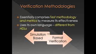
Functional Verification
Functional verification is performed through methods like simulation (RTL, gate-level, and post-layout) and formal verification techniques such as model checking, equivalence checking, and property checking. Random simulation broadens the scope, uncovering edge cases which traditional methods may overlook.
Timing Verification
Timing verification ensures that designs function correctly at the desired speed without timing violations. Techniques include Static Timing Analysis (STA), which computes delays without simulation, ensuring timing constraints are met, and analysis of clock tree characteristics for clock skews.
Both areas use specific algorithms like equivalence checking for functional verification and delay propagation algorithms for timing. Hybrid approaches integrating both methods are increasingly important in handling the complexity of modern designs. Challenges arise from design size, complexity, and multilayer designs, demanding advanced algorithms for efficient verification.
Youtube Videos
Audio Book
Dive deep into the subject with an immersive audiobook experience.
Introduction to VLSI Verification
Chapter 1 of 10
🔒 Unlock Audio Chapter
Sign up and enroll to access the full audio experience
Chapter Content
Verification is a critical step in the VLSI design flow, ensuring that the design meets its functional and timing specifications. Verification algorithms are used to validate that the circuit behaves as intended and that it meets the required timing constraints. As VLSI designs become increasingly complex, verification has become one of the most time-consuming and challenging aspects of the design process.
Detailed Explanation
In VLSI (Very Large Scale Integration) design, verification is a crucial phase that ensures all aspects of the circuit design function as intended and meet preset specifications. This includes both the logical behavior (functional verification) and the timing constraints (timing verification) necessary for the circuit to operate correctly in a real-world scenario.
Examples & Analogies
Think of verification like preparing a vehicle for a race. Before the vehicle hits the track, you need to ensure that the engine runs smoothly (functional verification) and that all performance parameters, such as acceleration and braking time, fit within the rules of the race (timing verification). If any issue is found during this phase, it has to be addressed before the vehicle can safely compete.
Types of Verification
Chapter 2 of 10
🔒 Unlock Audio Chapter
Sign up and enroll to access the full audio experience
Chapter Content
There are two primary types of verification:
● Functional Verification: Ensures that the design behaves correctly according to the specifications.
● Timing Verification: Ensures that the design meets the required timing constraints, such as setup time, hold time, and clock frequency.
Detailed Explanation
The verification process in VLSI is divided into two main types: functional verification and timing verification. Functional verification checks whether the design implements the intended operations correctly based on specifications, while timing verification focuses on ensuring the design meets all timing-related requirements. Timing requirements include setup time (how early inputs need to be stable before a clock pulse) and hold time (how long the inputs must remain stable after a clock pulse).
Examples & Analogies
Imagine creating a recipe. Functional verification is like checking that you have all the ingredients and that they are used in the proper order. Timing verification, on the other hand, is like ensuring that you allow the right amount of time for each step, such as simmering a sauce for the correct duration without burning it.
Functional Verification in VLSI
Chapter 3 of 10
🔒 Unlock Audio Chapter
Sign up and enroll to access the full audio experience
Chapter Content
Functional verification aims to ensure that the design meets the intended functionality by checking that all operations of the circuit behave correctly. It involves simulating the design to verify that it performs as expected under various operating conditions.
Detailed Explanation
Functional verification entails simulating the VLSI design to validate that all operations are executed correctly under different conditions. This is essential because even minor mistakes in the design could lead to significant operational failures. The simulation helps discover bugs and issues before physical prototypes are built.
Examples & Analogies
Think of functional verification as rehearsing a play. The actors (the circuit design) go through their lines and actions (operations) to ensure everything is performed correctly before the actual show (the final product). Each rehearsal helps identify mistakes and improves performance.
Methods of Functional Verification
Chapter 4 of 10
🔒 Unlock Audio Chapter
Sign up and enroll to access the full audio experience
Chapter Content
Functional verification is typically performed using the following methods:
● Simulation: Running a simulation of the design using input vectors to check the output of the circuit. It can be done at various levels of abstraction:
○ RTL Simulation: Verifying the Register Transfer Level (RTL) description of the design using testbenches.
○ Gate-Level Simulation: Simulating the synthesized gate-level netlist to verify functionality after synthesis.
○ Post-Layout Simulation: Verifying the circuit after layout and routing to ensure functionality after physical design.
Detailed Explanation
Functional verification employs several simulation methods to test the circuit at different design stages. RTL simulation checks the design at a high level using testbenches, gate-level simulation examines the implementation after synthesis, and post-layout simulation confirms that the design still works correctly after the physical layout has been applied.
Examples & Analogies
This can be compared to different stages of a product development process. Initially, you might test a concept using a prototype (RTL simulation). Once the design is finalized, you create a more refined version (gate-level simulation) and finally build a complete operational model (post-layout simulation) to ensure everything works as intended before mass production.
Formal Verification Techniques
Chapter 5 of 10
🔒 Unlock Audio Chapter
Sign up and enroll to access the full audio experience
Chapter Content
Formal Verification: This method uses mathematical proofs to verify that the design satisfies its specifications. Formal methods involve checking that the design's behavior, as specified by the HDL code, is logically correct and consistent. Formal verification techniques include:
● Model Checking: Automatically verifying that a design satisfies certain properties (e.g., safety or liveness properties) by exhaustively checking all possible states.
● Equivalence Checking: Ensuring that the RTL design and its corresponding gate-level implementation are functionally equivalent.
● Property Checking: Verifying that specific properties (e.g., functional behavior, safety conditions) hold true throughout the design.
Detailed Explanation
Formal verification uses rigorous mathematical methods to prove that the circuit design adheres to its specifications. This can involve checking that the design is safe (won't produce harmful outputs) and that it performs correctly under all possible conditions. Techniques like model checking explore every possible state of the system to ensure safety and performance.
Examples & Analogies
This process is similar to a lawyer preparing a case for court. Just as a lawyer must present irrefutable evidence and logic to prove their arguments, formal verification provides mathematical proof that the design meets all requirements, ensuring there are no overlooked conditions or scenarios.
Timing Verification in VLSI
Chapter 6 of 10
🔒 Unlock Audio Chapter
Sign up and enroll to access the full audio experience
Chapter Content
Timing verification is essential to ensure that the design operates at the intended speed and meets the timing constraints. The goal is to verify that the design can operate correctly at the desired clock frequency without encountering setup or hold violations.
Detailed Explanation
Timing verification checks whether a VLSI design meets its speed requirements and performs reliably without timing violations. This process ensures that the design can work correctly at the intended clock frequency, avoiding issues where signals do not settle in time for the next operational clock edge.
Examples & Analogies
Consider a relay race where teammates pass the baton. Timing verification is like ensuring that each runner (circuit component) knows exactly when to hand off the baton (data signal) to the next runner without dropping it (timing violations). If any handoff is too early or too late, it can lead to failure in completing the race.
Static Timing Analysis (STA)
Chapter 7 of 10
🔒 Unlock Audio Chapter
Sign up and enroll to access the full audio experience
Chapter Content
Static Timing Analysis (STA): STA is a method used to verify whether the timing constraints of the design are met without the need for simulation. It checks the delay of all signal paths in the design and ensures that there are no timing violations, such as setup or hold violations.
Detailed Explanation
Static Timing Analysis (STA) evaluates all signal paths in a design to confirm that all timing constraints are satisfied, without the need for running complex simulations. STA looks at the maximum delays and ensures that they don’t exceed the specified timing requirements, allowing designers to identify potential issues early in the design phase.
Examples & Analogies
Envision a train schedule where it is essential to ensure that trains leave and arrive at their stations on time. STA works similarly by checking the timing of each segment of the train's journey to make sure it complies with the overall schedule and avoids delays.
Clock Tree Analysis
Chapter 8 of 10
🔒 Unlock Audio Chapter
Sign up and enroll to access the full audio experience
Chapter Content
Clock Tree Analysis: This is part of timing verification where the clock tree, which distributes the clock signal across the design, is analyzed to ensure that all flip-flops receive the clock signal at the correct time. The goal is to minimize clock skew and ensure that the clock signal arrives simultaneously at all flip-flops.
Detailed Explanation
Clock Tree Analysis focuses on ensuring that the clock signal reaches all components in a synchronized manner. A properly tuned clock tree minimizes clock skew, which can lead to timing violations if different components receive the clock signal at different times, essentially ensuring that every part of the circuit operates in harmony.
Examples & Analogies
This can be compared to an orchestra. Just as all musicians must start their notes at the exact moment the conductor signals to ensure a harmonious performance, clock tree analysis ensures that each flip-flop receives the clock signal at the same time, enabling the circuit to function seamlessly.
Challenges in Verification
Chapter 9 of 10
🔒 Unlock Audio Chapter
Sign up and enroll to access the full audio experience
Chapter Content
As VLSI designs grow more complex, verification becomes increasingly difficult due to:
● Design Size: The larger the design, the more difficult it is to verify every possible behavior.
● Complexity of Timing Analysis: With multiple clock domains and high-frequency circuits, verifying timing constraints can become computationally expensive and time-consuming.
● Verification of Multilayer Designs: Advanced designs with multiple layers of interconnects and complex routing require sophisticated verification algorithms to ensure that all layers work correctly together.
Detailed Explanation
As VLSI designs expand in size and complexity, verification processes face significant challenges. Larger designs can lead to unmanageable numbers of possible scenarios to test. Moreover, high-frequency circuits often involve multiple clock domains, complicating the timing analysis. Finally, multilayer designs introduce additional layers of routing and connections that must also be verified for integrated functionality.
Examples & Analogies
Think of these challenges as managing a large event. The more attendees (design components), the more coordination is needed to ensure every aspect functions correctly. Timing becomes complicated if there are multiple events (clock domains) happening at once, and ensuring everything runs smoothly through multiple rooms (layers of interconnections) requires extensive planning and oversight.
Conclusion of Verification in VLSI
Chapter 10 of 10
🔒 Unlock Audio Chapter
Sign up and enroll to access the full audio experience
Chapter Content
Verification is an essential step in the VLSI design flow, ensuring that the circuit functions as expected and meets timing constraints. Functional verification guarantees that the design operates correctly under various conditions, while timing verification ensures that the design can operate at the desired clock speed without timing violations. Verification algorithms, including simulation-based methods, formal methods, and static timing analysis, are crucial for validating large and complex VLSI designs.
Detailed Explanation
In summary, verification stands as a cornerstone of the VLSI design process. Ensuring the correctness of designs through functional and timing verification is crucial for producing reliable circuits. Various verification algorithms and methodologies enable designers to validate their complex designs effectively, highlighting the growing importance of sophisticated verification methods as technology evolves.
Examples & Analogies
This conclusion can be likened to quality assurance in manufacturing. Just like products undergo rigorous testing to ensure they function correctly before reaching consumers, VLSI designs must pass through thorough verification stages to guarantee their reliability and performance in real-world applications.
Key Concepts
-
Verification in VLSI: The process of confirming that a design meets its intended specifications for functionality and timing.
-
Functional Verification: Methods used to check that the design operates correctly according to its specifications.
-
Timing Verification: Methods to ensure that the design meets all timing constraints necessary for its correct functionality.
-
Static Timing Analysis (STA): A technique used to analyze the timing of circuits without extensive simulation, focusing on signal delays through the design.
Examples & Applications
A circuit design undergoes functional verification through simulations at the RTL, ensuring that the outputs match the expected results for given inputs.
Static Timing Analysis is used for a high-speed digital circuit to ensure that setup and hold times are met, preventing data corruption.
Memory Aids
Interactive tools to help you remember key concepts
Rhymes
When circuits design, we must test on a dime, verifying all codes, in proper timing is prime.
Stories
Imagine a wizard who casts spells (tests) on designs to ensure they work perfectly. Each spell must match the intended effect (function), and the timing of each puff of magic must be just right or disaster will strike!
Memory Tools
To remember the verification types: 'FAT': Functional checks, Analysis for timing, and Test the environment.
Acronyms
STA for Static Timing Analysis keeps your circuit on time, ensuring every signal path can function just fine.
Flash Cards
Glossary
- VLSI
Very Large Scale Integration, referring to the process of creating integrated circuits by combining thousands of transistors into a single chip.
- Functional Verification
The process of checking that the design functions according to its specifications.
- Timing Verification
The process of ensuring that the design meets all timing constraints.
- Static Timing Analysis (STA)
A method of verifying timing constraints by analyzing signal delays without requiring full simulation.
- Testbench
A virtual environment used to simulate the behavior of a design and apply test stimuli for verification.
- Model Checking
A formal verification method for checking model properties through exhaustive state exploration.
- Equivalence Checking
A verification method that ensures two designs behave equivalently after transformations.
Reference links
Supplementary resources to enhance your learning experience.