
Altium Designer, KiCad, OrCAD
Interactive Audio Lesson
Listen to a student-teacher conversation explaining the topic in a relatable way.
Introduction to PCB Design Tools
🔒 Unlock Audio Lesson
Sign up and enroll to listen to this audio lesson

Today, we’re discussing crucial tools for PCB design: Altium Designer, KiCad, and OrCAD. Why do you think these tools are vital in the design process?

I think they're important because they help structure the layout correctly.
Exactly! They provide a structured way to visualize how circuit components will be arranged. Let's remember this with the acronym **ASK** - Altium, KiCad, and OrCAD. Can anyone explain what each of these tools is primarily used for?

Altium Designer is known for its advanced features, right?

KiCad is free and open-source, I believe!

OrCAD is known for simulating electrical behavior in circuits.
Great! To recap, Altium is robust for professional use, KiCad offers accessibility, and OrCAD excels in simulation capabilities.
Architectural Annotation in Design Tools
🔒 Unlock Audio Lesson
Sign up and enroll to listen to this audio lesson

Now, let's talk about architectural annotations. Why do they matter in PCB design?
They help clarify how components interact and fit into the larger system.
Exactly, and they improve team communication. Remember the phrase **'See the big picture!'** can help us remember this aspect. Can anyone share what features contribute to annotations in these tools?
I think they allow us to connect various elements visually.
They also help in documentation for future reference.
Spot on! Clear documentation is key for ongoing projects. In summary, architectural annotations enhance both clarity and functionality in the design.
Comparative Analysis of PCB Design Tools
🔒 Unlock Audio Lesson
Sign up and enroll to listen to this audio lesson
Let’s compare the three tools. What are key differences that come to mind?
Altium Designer is typically used in commercial settings, while KiCad is more for hobbyists.
OrCAD is often used in industries that require robust simulation.
Exactly! Altium is professional and feature-rich, whereas KiCad provides an accessible entry point without cost. Both Altium and OrCAD excel in advanced simulation capabilities. To keep this straight, think of the acronym **A-K-O** - Altium, KiCad, OrCAD for their typical user base.
So, if you're working on a budget, KiCad is the way to go.
Perfect! Summary points to take away: Altium for features, KiCad for cost-effective solutions, and OrCAD for its simulation strengths.
Introduction & Overview
Read summaries of the section's main ideas at different levels of detail.
Quick Overview
Standard
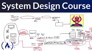
The section discusses three popular PCB design tools: Altium Designer, KiCad, and OrCAD. It highlights how these tools facilitate schematic and PCB design while allowing for architectural annotation that supports system-level design and analysis.
Detailed
Altium Designer, KiCad, OrCAD
This section focuses on essential tools utilized in hardware architecture and modeling, specifically detailing three significant software tools for PCB design: Altium Designer, KiCad, and OrCAD. These tools are pivotal for engineers seeking to create detailed electronic schematics and printed circuit boards (PCBs) while incorporating architectural annotations that enhance the design process.
Key Points:
- Application in PCB Design: Each tool serves as a comprehensive platform for designing schematics and PCBs, offering a variety of features tailored for optimizing the electronic design process.
- Architectural Annotation: They support integration of architectural elements into the design, allowing designers to align circuit board layouts with higher-level system architectures. This can lead to enhanced communication within design teams and more structured project development.
- Interconnectivity: These tools not only create designs but also ensure that various components work seamlessly together within a larger system architecture.
Understanding the capabilities of these tools is crucial for engineers who aim to implement effective designs that meet both functional and performance specifications.
Youtube Videos

Audio Book
Dive deep into the subject with an immersive audiobook experience.
Overview of Design Tools
Chapter 1 of 4
🔒 Unlock Audio Chapter
Sign up and enroll to access the full audio experience
Chapter Content
- Altium Designer, KiCad, OrCAD: Schematic and PCB design with architectural annotation
Detailed Explanation
This overview highlights three popular software tools used in electronic design automation. Altium Designer, KiCad, and OrCAD are utilized for creating schematic diagrams and Printed Circuit Board (PCB) layouts. These tools allow engineers to annotate their designs with architectural notes, which help in understanding the functionality and components of the design more clearly.
Examples & Analogies
Think of these tools like software for architects who design buildings. Just like architects use software to create blueprints and add annotations to explain the various parts of a construction plan, electronic engineers use Altium Designer, KiCad, and OrCAD to create detailed diagrams that represent the circuitry of electronic devices.
Schematic Design
Chapter 2 of 4
🔒 Unlock Audio Chapter
Sign up and enroll to access the full audio experience
Chapter Content
Schematic design involves creating a visual representation of the electronic components and their interconnections.
Detailed Explanation
In schematic design, engineers draw symbols representing various electronic components, such as resistors, capacitors, and microcontrollers. Lines are used to connect these components, showing how they communicate and work together. This technical drawing acts like a blueprint for a house, indicating where each room (or component) is located and how they are all linked.
Examples & Analogies
Imagine you are creating a map for a treasure hunt. Each landmark (like a tree or rock) represents a component, and the paths between them represent the connections. Similarly, in schematic design, the components and their connections are mapped out visually to ensure proper functioning.
PCB Layout Design
Chapter 3 of 4
🔒 Unlock Audio Chapter
Sign up and enroll to access the full audio experience
Chapter Content
PCB layout design translates the schematic into a physical board layout, defining component placement and routing of connections.
Detailed Explanation
Once the schematic is complete, the next step is to design the PCB layout. This involves determining how components will be physically arranged on the board and creating paths (or traces) for electrical connections between components. The goal is to optimize space, minimize signal interference, and ensure effective electrical performance.
Examples & Analogies
Consider a game of Tetris. Each block represents an electronic component. Your job is to fit all the blocks together in a limited space while ensuring that they connect properly and create a solid foundation for your 'game.' The PCB layout does the same for electronic components, fitting them onto a board in an efficient arrangement.
Architectural Annotation
Chapter 4 of 4
🔒 Unlock Audio Chapter
Sign up and enroll to access the full audio experience
Chapter Content
Architectural annotation enhances schematics and layouts with detailed information related to design intent and specifications.
Detailed Explanation
Architectural annotation is the process of adding notes and information to the schematic and PCB layout designs. This documentation includes specifications, design rationale, and guidelines, which help ensure that anyone working with the design can understand its structure and purpose. This can be crucial when collaborating with other engineers or during future revisions.
Examples & Analogies
Think of this like writing the instructions for assembling a piece of IKEA furniture. The instructions not only show you what the final piece should look like but also provide important tips and warnings. Similarly, architectural annotations explain how to put the electronic design together correctly and highlight any specific considerations to keep in mind.
Key Concepts
-
PCB Design Tools: Software essential for creating electronic schematics and PCBs.
-
Architectural Annotation: Enhancements in communication and design through detailed documentation.
Examples & Applications
Using Altium Designer enables detailed multilevel schematics that facilitate complex PCB layouts.
KiCad can be used to create simple designs without high costs, particularly beneficial for educational projects.
Memory Aids
Interactive tools to help you remember key concepts
Rhymes
Altium's got the might, for pro designs that fit just right.
Stories
Imagine a hobbyist named Kay who builds circuits each day. With KiCad in hand, creativity expands, making projects not just a cliché.
Memory Tools
Remember A-K-O: Altium, KiCad, OrCAD for professional, hobbyist, and simulation use.
Acronyms
Use **PCB** for the processes
Plan
Create
Build.
Flash Cards
Glossary
- Altium Designer
A professional PCB design software known for its advanced features and capabilities.
- KiCad
An open-source PCB design tool that provides an accessible option for hobbyists and professionals.
- OrCAD
A PCB design tool known for its simulation capabilities, widely used in industry.
Reference links
Supplementary resources to enhance your learning experience.