
Digital Circuit Design and Implementation on FPGAs
Enroll to start learning
You’ve not yet enrolled in this course. Please enroll for free to listen to audio lessons, classroom podcasts and take practice test.
Interactive Audio Lesson
Listen to a student-teacher conversation explaining the topic in a relatable way.
Introduction to Digital Circuit Design
🔒 Unlock Audio Lesson
Sign up and enroll to listen to this audio lesson

Digital circuits play a key role in electronic systems. Can anyone share why flexibility is vital in these designs?

I think flexibility allows for changes without needing new hardware.
Exactly! FPGAs enable this flexibility, allowing for updates after deployment. This leads us to consider the design flow.
Understanding the Design Flow for FPGA-Based Systems
🔒 Unlock Audio Lesson
Sign up and enroll to listen to this audio lesson

The design flow comprises several critical stages. Can anyone name one of these stages?

Design Specification!
Correct! We start by defining the problem and functionality. What's next after writing the specification?

I believe it's Hardware Description?
Right again! We write our design in VHDL or Verilog. This leads into our next crucial step, simulation.
Simulation and Verification
🔒 Unlock Audio Lesson
Sign up and enroll to listen to this audio lesson
After creating our design, we simulate it to check for errors. Why do you think this step is essential?

It helps catch mistakes before going to hardware!
Exactly! A testbench is created to verify functionality. Can anyone give me an example of what we might test?
Input and output correctness!
Writing VHDL and Verilog Code
🔒 Unlock Audio Lesson
Sign up and enroll to listen to this audio lesson
Once the design is specified, we write the code. What is a critical part of this coding process?
Entity or module definition! It's important to declare inputs and outputs.
Exactly, great point! Let's look at a practical example, like writing a 4-bit adder.
Introduction & Overview
Read summaries of the section's main ideas at different levels of detail.
Quick Overview
Standard
The section outlines the workflow of designing digital circuits on FPGAs, emphasizing the importance of comprehensive design specifications, the process of coding in VHDL or Verilog, and the stages from simulation to programming the FPGA.
Detailed
Digital Circuit Design and Implementation on FPGAs
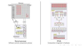
In this chapter, we delve into the process of designing and implementing digital circuits on Field-Programmable Gate Arrays (FPGAs). FPGAs are flexible and capable of parallel processing, making them a vital tool for both simple and intricate circuit designs.
Key Highlights:
- Design Flow: The design flow includes several stages such as:
- Design Specification: Identify the problem and functionality, defining inputs and outputs clearly.
- Hardware Description: Use VHDL or Verilog to describe the design.
- Simulation: Validate the design to identify and correct errors.
- Synthesis: Convert descriptions into a netlist of logical gates.
- Implementation: Map the synthesized design onto FPGA resources.
- Verification: Ensure functionality through testbenches.
- Programming: Generate and load the configuration bitstream into the FPGA.
- Testing and Debugging: Final checks and adjustments to ensure performance.
The detailed sections present a real-world example, such as the implementation of a 4-bit binary adder, showcasing how to translate high-level designs into code, simulate, and verify circuit functionality before actual hardware implementation.
Youtube Videos

Audio Book
Dive deep into the subject with an immersive audiobook experience.
Introduction to Digital Circuit Design on FPGAs
Chapter 1 of 7
🔒 Unlock Audio Chapter
Sign up and enroll to access the full audio experience
Chapter Content
Digital circuits are the backbone of modern electronic systems, enabling everything from simple logic functions to complex signal processing. Field-Programmable Gate Arrays (FPGAs) provide an ideal platform for designing and implementing these circuits due to their flexibility, parallel processing capabilities, and high-speed performance. This chapter introduces the process of digital circuit design and implementation on FPGAs using VHDL and Verilog. We will cover the steps required to translate design specifications into functional systems on an FPGA, from conceptualization and simulation to implementation and verification. Additionally, we will discuss practical tips for optimizing designs and improving performance.
Detailed Explanation
This chunk provides an overview of what digital circuits are and why FPGAs are suitable for their design and implementation. Digital circuits are fundamental components in electronics, being used in everything from calculators to complex computers. FPGAs are integrated circuits that can be configured after manufacturing, allowing designers to customize their hardware for specific tasks. This section sets the stage for the following topics by highlighting the importance of understanding the design and implementation process, which includes using hardware description languages like VHDL and Verilog.
Examples & Analogies
Think of digital circuits like recipes in a cookbook. Just as you follow a recipe to create a dish, digital circuit designers follow specifications to create functionalities for electronic devices. FPGAs act like chefs who can prepare various dishes based on different recipes, allowing them to adapt quickly to new culinary trends (or technological needs) without needing to start from scratch.
Understanding the Design Flow for FPGA-Based Systems
Chapter 2 of 7
🔒 Unlock Audio Chapter
Sign up and enroll to access the full audio experience
Chapter Content
The design flow for FPGA-based systems consists of several stages that ensure the correct implementation of a digital circuit. These stages include: 1. Design Specification: - Define the problem and the required functionality. - Create a detailed description of the digital circuit, including its inputs, outputs, and behavior. 2. Hardware Description: - Write the design using VHDL or Verilog to describe the circuit’s behavior and structure. 3. Simulation: - Simulate the design to verify its functionality and check for any errors in the behavior or performance. 4. Synthesis: - Convert the hardware description into a netlist that represents the logical gates and components to be implemented on the FPGA. 5. Implementation: - Map the synthesized design to the FPGA architecture, considering constraints like timing and resource usage. 6. Verification: - Verify the design's functionality on the actual FPGA using testbenches and real-world stimulus. 7. Programming the FPGA: - Generate the configuration bitstream and program the FPGA to implement the design. 8. Testing and Debugging: - Test the FPGA-based system, troubleshoot any issues, and make necessary modifications.
Detailed Explanation
This chunk outlines the step-by-step design flow involved when creating digital circuits for FPGAs. The process begins with defining what the circuit needs to do (design specification) and moves through various stages including writing the design in a hardware description language, simulating it to catch any errors, synthesizing the design into a format the FPGA can understand, implementing it on the FPGA, and finally testing it in real-world conditions. Each stage builds upon the previous one, ensuring an organized approach to circuit design and implementation.
Examples & Analogies
Consider this design flow like building a house. You start with planning (design specification), then you draw up the blueprints (hardware description). Before construction starts, you might build a miniature model (simulation) to ensure everything fits well. Once satisfied with the plans, you gather materials (synthesis) and begin building (implementation). After the house is built, you conduct a walkthrough (verification) to check for flaws before moving in (programming and testing). This systematic approach helps catch errors early and ensures the final product is safe and functional.
Design Specification and Requirements
Chapter 3 of 7
🔒 Unlock Audio Chapter
Sign up and enroll to access the full audio experience
Chapter Content
The first step in designing any digital circuit on an FPGA is to understand the functional requirements. The design specification should outline the circuit's functionality, input/output interfaces, and timing constraints. Example: 4-Bit Binary Adder Design Specification: ● Inputs: Two 4-bit binary numbers (A and B) and a carry input (Cin). ● Outputs: A 4-bit sum (S) and a carry output (Cout). ● Functionality: The circuit adds the two binary numbers along with the carry input and outputs the sum and carry output. This simple example will help demonstrate the process of translating a high-level design into FPGA code.
Detailed Explanation
In this chunk, the focus is on the critical first step of designing digital circuits: understanding what the circuit must achieve. This involves detailing the inputs, outputs, and the behavior of the circuit in various conditions. An example is provided to clarify this concept—a 4-bit binary adder, which shows how specifics are laid out to guide the subsequent steps of coding and implementation.
Examples & Analogies
Think of designing a new electronic toy. Before building it, you need to decide how it will work (functional requirements), what pieces it will need (inputs and outputs), and how fast it should respond (timing constraints). By preparing these specifications carefully, you can ensure that your toy will function correctly and provide the entertainment you envisioned, just like a well-defined circuit ensures it behaves as intended.
Writing the VHDL/Verilog Code for FPGA Implementation
Chapter 4 of 7
🔒 Unlock Audio Chapter
Sign up and enroll to access the full audio experience
Chapter Content
Once the design specifications are clear, the next step is to describe the circuit using VHDL or Verilog. The code must include the entity/module definition, port declarations, and logic to implement the desired functionality.
Detailed Explanation
This chunk discusses the next phase after defining the design specifications: coding the design with a hardware description language such as VHDL or Verilog. The code should effectively express the circuit's structure and behavior, detailing the connections and functions of its components. This phase is crucial as it translates the idea from a conceptual description into a specific format the FPGA can understand.
Examples & Analogies
Writing VHDL or Verilog code is like writing the instruction manual for assembling model furniture. Just as the manual provides step-by-step instructions and diagrams to build the furniture correctly, the code provides the detailed information needed for the FPGA to create the desired circuit functionality.
Simulation and Verification
Chapter 5 of 7
🔒 Unlock Audio Chapter
Sign up and enroll to access the full audio experience
Chapter Content
Before implementing the design on the FPGA, it is important to verify the functionality of the digital circuit using simulation. Simulating the design helps detect logic errors, race conditions, or timing violations early in the process.
Detailed Explanation
Here, the focus is on the importance of simulation as a crucial step in confirming the design's functionality before actual implementation. By simulating the circuit, designers can identify potential errors such as bugs or timing issues, allowing them to make corrections before the circuit is deployed on the FPGA, which can save time and resources.
Examples & Analogies
Think of simulating your design like taking a practice test before the actual exam. Just as a practice test helps highlight areas where you need improvement and allows you to fix mistakes before the real test, circuit simulation helps uncover potential faults in design, allowing you to resolve them without the costs associated with physical prototyping.
Synthesis and Implementation
Chapter 6 of 7
🔒 Unlock Audio Chapter
Sign up and enroll to access the full audio experience
Chapter Content
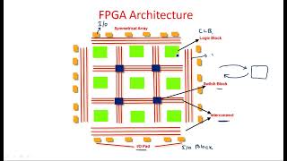
After successfully simulating the design and ensuring its correctness, the next step is synthesis. The synthesis tool converts the hardware description into a netlist, mapping the design onto the FPGA's resources (logic blocks, I/O, etc.). - Synthesis Tools: Vivado (Xilinx), Quartus (Intel), or other FPGA vendor-specific tools. - Implementation: The synthesis tool performs placement and routing of the design, ensuring that the logic is correctly mapped to the FPGA.
Detailed Explanation
This chunk covers the synthesis phase, where the software takes the hardware description code and converts it into a netlist—essentially a map of how the design will be built in the FPGA's architecture. Following this, the implementation process involves placing the different components correctly on the FPGA and routing the connections to ensure everything works as intended.
Examples & Analogies
Synthesis and implementation can be compared to a construction project where architects (designers) create detailed blueprints (the netlist) for building a house (the FPGA). The builders (synthesis tools) then take these blueprints to determine where to place each room and hallway (placement) and how to connect them (routing), ensuring that the entire house is functional and up to code.
Conclusion
Chapter 7 of 7
🔒 Unlock Audio Chapter
Sign up and enroll to access the full audio experience
Chapter Content
This chapter covered the fundamentals of digital circuit design and implementation on FPGAs, focusing on how to translate design specifications into functional systems using VHDL and Verilog. You learned how to define, simulate, synthesize, and implement digital circuits on FPGA platforms. By practicing these concepts, you will gain the skills necessary to design more complex FPGA systems and contribute to real-world digital solutions.
Detailed Explanation
In the concluding chunk, the chapter summarizes the key takeaways regarding FPGA-based digital circuit design. It reiterates the importance of understanding the complete process from specifications to implementation, illustrating how this knowledge builds a foundation for more advanced projects and skills needed in the field of electronics.
Examples & Analogies
Think of this conclusion as the final chapter of a journey. Every step you've learned, from mapping the landscape of circuit design to navigating challenges in programming the FPGA, prepares you for more ambitious ventures in the electronics world, much like how every hike prepares an adventurer for an even taller mountain in the future.
Key Concepts
-
Design Specification: The initial definition of circuit requirements including inputs, outputs, and functionality.
-
Simulation: The phase where the digital design is tested through a virtual environment to ensure correctness.
-
VHDL/Verilog: Hardware description languages used for coding FPGA designs.
Examples & Applications
A practical implementation of a 4-bit binary adder, showcasing how inputs and outputs translate into functional FPGA codes.
Using a testbench to validate the 4-bit adder by providing different inputs and checking the outputs.
Memory Aids
Interactive tools to help you remember key concepts
Rhymes
For an FPGA, the circuits come to play, with flexibility every day!
Stories
Imagine designing a race car; you sketch the model, simulate its speed, and after confirming it can win the race, it's built for real on the track - that's like designing with FPGAs.
Memory Tools
F-PGA Design Flow: 'S-Simulate, S-Synthesize, I-Implement, T-Test!'
Acronyms
SYNTHESIS
S-Specification
Y-Yield Term
N-Netlist
T-Testbench
H-Implementation
E-Errors caught
S-Simulation
I-Integration
S-Success confirmed.
Flash Cards
Glossary
- FPGA
Field-Programmable Gate Array, a hardware device that can be configured by the user to perform specific functions.
- VHDL
VHSIC Hardware Description Language, a language used to describe the behavior and structure of electronic systems.
- Verilog
A hardware description language used for modeling electronic systems.
- Testbench
A simulated environment used to verify the functionality of a digital circuit.
- Synthesis
The process of converting a hardware description into a netlist that can be implemented on an FPGA.
Reference links
Supplementary resources to enhance your learning experience.