
Implementation
Enroll to start learning
You’ve not yet enrolled in this course. Please enroll for free to listen to audio lessons, classroom podcasts and take practice test.
Interactive Audio Lesson
Listen to a student-teacher conversation explaining the topic in a relatable way.
Introduction to Implementation
🔒 Unlock Audio Lesson
Sign up and enroll to listen to this audio lesson

Today we're diving into the implementation phase of FPGA design. After synthesis, we need to properly map our designs to the specific FPGA architecture. Can anyone summarize what the synthesis phase entails?

Synthesis converts our code into a netlist, which is a representation of the logical gates.
Exactly! So, the implementation phase is where we take that netlist and use FPGA resources. Why do you all think this step is critical?

If we don't properly map it, our design won't work correctly on the FPGA.
Right! Mapping ensures that all components fit and work efficiently. Remember the acronym 'MAP': **M**ap, **A**llocate, **P**rogram. Let's define each of these steps.
Mapping the Design
🔒 Unlock Audio Lesson
Sign up and enroll to listen to this audio lesson

Now let's talk about mapping the synthesized design. Why do we need to consider timing constraints during this phase?

If the timing isn't right, the signals can interfere with each other, causing errors.
Correct! We need to ensure signals propagate correctly within their timing specs. Any other factors we should consider?

Resource usage affects how many logic elements we can utilize without exceeding the FPGA capacity.
Excellent point! The balance between speed, area, and power is crucial. This is the balance we strive for during mapping to optimize the design performance.
Generating Configuration Bitstream
🔒 Unlock Audio Lesson
Sign up and enroll to listen to this audio lesson
After we map our design, the next step is creating a configuration bitstream. Can anyone explain its significance?
The bitstream configures the FPGA to perform the functions we designed!
Exactly! This file is crucial for programming the FPGA. What might happen if there's an issue in generating the bitstream?
The FPGA won't operate correctly, and our design could fail.
Right. Hence, it's important to validate this process. Remember to always check constraints during implementation. Let’s do a recap!
Understanding Timing and Resource Constraints
🔒 Unlock Audio Lesson
Sign up and enroll to listen to this audio lesson
Before we wrap up, let’s discuss timing and resource constraints. Can someone give me a reason why managing resources is essential?
If we exceed resources, parts of our design may not fit on the FPGA!
Correct! Let’s not forget timing. Who can summarize how we might check for timing issues?
We can use timing analysis tools to ensure all paths meet their required timing closure.
Exactly! Monitoring constraints during every stage ensures designs are successful. Well done today, everyone!
Introduction & Overview
Read summaries of the section's main ideas at different levels of detail.
Quick Overview
Standard
In this section, we discuss the implementation stage in the FPGA design flow, which involves mapping synthesizable designs to physical FPGA elements, meeting timing and resource constraints, and programming the FPGA with a configuration bitstream to execute the designed functionality.
Detailed
Implementation in FPGA Design Flow
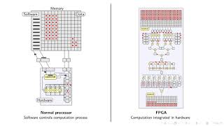
In this section, we explore the critical implementation phase in the FPGA design flow after synthesis. Once the hardware description is synthesized into a netlist, the implementation process is initiated, characterized by two primary activities: Mapping and Configuration.
Key Steps in Implementation
- Mapping the Design: The objective of this step is to efficiently assign design elements from the netlist to the specific resources of the FPGA. This involves strategically placement of logical blocks, optimizing for speed, area, and power consumption. The implementation tools automatically determine how the logical circuits can best utilize the available physical resources while satisfying performance constraints and limitations.
- Configuration: After mapping is completed, the next step is to generate a configuration bitstream. This file encodes the specific configuration of the FPGA, defining how elements are interconnected to fulfill the design objectives as specified in the original design documentation. The bitstream is critical since it enables the FPGA to operate as intended once programmed.
Constraints Management
During implementation, designers must manage various constraints, such as timing constraints (ensuring data signals meet their timing specifications) and resource usage (making sure the design occupies the physical resources available on the FPGA). The tools provide options to fine-tune these settings.
Conclusion
Implementing a design onto an FPGA requires a carefully guided approach, ensuring logical constructs are optimally represented on the architecture. Understanding this process is essential for successful FPGA development, improving reliability and performance of digital circuits.
Youtube Videos


Audio Book
Dive deep into the subject with an immersive audiobook experience.
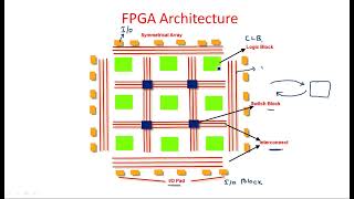
Mapping to FPGA Architecture
Chapter 1 of 2
🔒 Unlock Audio Chapter
Sign up and enroll to access the full audio experience
Chapter Content
○ Map the synthesized design to the FPGA architecture, considering constraints like timing and resource usage.
Detailed Explanation
This step involves taking the netlist generated from the synthesis phase and aligning it with the specific architecture of the FPGA being used. The goal is to ensure that the design functions correctly within the hardware limits of the FPGA. Designers must consider various constraints such as timing—ensuring signals propagate through the circuit in the required time—and resource usage—making sure the FPGA has enough logic blocks and I/O pins available. This process is crucial because even a well-designed circuit can fail if it is not correctly mapped to the FPGA's structure.
Examples & Analogies
Think of this step as arranging furniture in a room. Just as you need to consider the size of the room and the dimensions of each piece of furniture to ensure everything fits well, in FPGA design, you must consider the specific resources available in the FPGA and the timing requirements to arrange your circuit effectively.
Resource Usage Considerations
Chapter 2 of 2
🔒 Unlock Audio Chapter
Sign up and enroll to access the full audio experience
Chapter Content
○ Consider resource usage like timing and resource usage.
Detailed Explanation
When mapping the design to the FPGA, it's essential to monitor how many logic gates, registers, and other resources will be utilized. Each FPGA has a finite number of these resources, and exceeding the limits can lead to design failure. Timing constraints are also crucial; they determine how fast signals can travel through the circuits. If the design does not meet these timing requirements, it may not work as intended, leading to malfunctioning behavior of the digital circuit.
Examples & Analogies
Imagine trying to pack for a trip. You have a limited luggage space (the FPGA's resources), and you need to make sure that you include only the items you really need (the logic elements). If you try to fit too much in your luggage, some things won’t fit, just like a circuit that uses more resources than what the FPGA can provide. In addition, you have to plan your trip carefully to ensure you arrive on time (timing), just like ensuring your signals within the FPGA circuit meet their timing requirements.
Key Concepts
-
Mapping: The process of assigning netlist components to physical FPGA resources.
-
Configuration Bitstream: The encoded file that dictates FPGA functionality after programming.
-
Timing Constraints: Guidelines ensuring signals meet timing requirements for reliable operation.
-
Resource Usage: Management of available FPGA resources to ensure design feasibility.
Examples & Applications
Using a synthesis tool like Vivado, determine the placement of your components and generate a bitstream for programming an FPGA.
Adjusting timings within the design constraints can improve performance and prevent setup or hold time violations.
Memory Aids
Interactive tools to help you remember key concepts
Rhymes
To map and program, you see, bits define the FPGA's decree.
Stories
Imagine an architect, mapping a building. Each room must fit and function well, just like placing components on an FPGA.
Memory Tools
Think 'MRC' for Mapping, Resource usage, and Constraints.
Acronyms
MAP
Mapping
Allocating
Programming.
Flash Cards
Glossary
- Mapping
The process of assigning digital circuit elements from a synthesized netlist to physical resources on an FPGA.
- Configuration Bitstream
A binary file that encodes the configuration settings of an FPGA to enable specific logic operations.
- Timing Constraints
Specifications that require signals to meet certain timing properties to ensure correct circuit operation.
- Resource Usage
The amount and types of FPGA resources utilized by a digital design, including logic blocks and I/O pins.
Reference links
Supplementary resources to enhance your learning experience.