
Integration of IP Cores and System-Level Design
Enroll to start learning
You’ve not yet enrolled in this course. Please enroll for free to listen to audio lessons, classroom podcasts and take practice test.
Interactive Audio Lesson
Listen to a student-teacher conversation explaining the topic in a relatable way.
Introduction to IP Cores
🔒 Unlock Audio Lesson
Sign up and enroll to listen to this audio lesson

Welcome class! Today, we'll explore IP cores. Can anyone tell me what an IP core is?

Isn't it a reusable module for specific functions in FPGA design?
Exactly! IP cores are pre-designed logic blocks that save time in development. They can handle various tasks like memory control or communication protocols. Remember, 'IP' stands for Intellectual Property!

What are the types of IP cores available?
Great question! There are two main types: hard IP cores and soft IP cores. Hard IP cores are fixed in the silicon for performance, while soft cores are HDL-defined and flexible.

Can you give examples of each?
Sure! Examples of hard IP cores include DSP blocks, while soft IP cores include UART and I2C controllers. Remember: HARD is for high stability and low latency, while SOFT signifies flexibility!

How do we decide which core to use?
We will cover that next. Selecting the right IP core is crucial based on functionality, performance, and resource utilization. Let’s keep these points in mind for our next discussion!
To recap, IP cores are essential for speeding up FPGA designs, classified into hard and soft with distinct applications. Any questions before we move on?
Integration Steps for IP Cores
🔒 Unlock Audio Lesson
Sign up and enroll to listen to this audio lesson

Now that we know about IP cores, let’s discuss how to integrate them into our designs. What do you think is the first step?
Selecting the right IP core?
Exactly! We need to identify our design requirements first. After that, we select cores that best meet those needs based on performance and resources.
How do we configure the selected cores?
Configuration involves fine-tuning parameters such as data width and clock frequency. Many FPGA design tools offer wizards for this process to simplify it.
And what’s next after configuration?
Next, we connect the IP cores to ensure they communicate correctly. Using system buses like Avalon or AXI is often recommended for effective data management.
Can you connect multiple cores at once?
Yes, connecting multiple cores in a modular design fosters easier management. Remember, design is like building with blocks; the right connections matter for stability!
So, to summarize, we start with selecting cores, then configure, and connect them. Can anyone give a brief overview of this process?
System-Level Design Concepts
🔒 Unlock Audio Lesson
Sign up and enroll to listen to this audio lesson
Let’s delve into system-level design concepts now. What do you think modular design means?
Is it about creating smaller, reusable blocks?
Correct! Modular design allows us to work with smaller entities, making debugging and maintainability much easier.
And how do communication protocols fit into this?
Communication protocols, like AXI and SPI, facilitate interaction between different subsystems, critical for overall system integrity.
What about timing constraints?
Timing constraints ensure all components sync correctly. They’re crucial for minimizing delays. Remember, time is money in design!
Could you summarize the key concepts of system-level design?
Absolutely! System-level design encompasses modular approaches, established communication protocols, and timing optimizations. These ensure our integrated cores function seamlessly together.
Best Practices for System-Level FPGA Design
🔒 Unlock Audio Lesson
Sign up and enroll to listen to this audio lesson
Finally, let's review some best practices for system-level FPGA design. What do you think should come first?
Planning the design architecture?
Exactly! A well-defined architecture guides all subsequent design efforts.
Why is it good to use high-level abstractions?
High-level abstractions let you prototype efforts quickly, enabling verification before diving into complex details. Think of it as sketching a rough draft before writing a complete essay!
Do we really need to test often?
Yes! Continuous testing ensures that issues are caught early, reducing the risk of complications later on in the process.
What about performance optimization?
After confirming functionality, optimizing resource use and timing can greatly enhance performance. Remember: optimized designs lead to better, faster systems!
To summarize, always plan architecture, use abstractions for prototypes, test often, and optimize for performance to achieve successful FPGA designs. Any questions?
Introduction & Overview
Read summaries of the section's main ideas at different levels of detail.
Quick Overview
Standard
The section highlights the importance of IP cores in FPGA design, covering their types, integration steps, and best practices for system-level design. Understanding these concepts is crucial for effectively developing and managing FPGA-based systems.
Detailed
Integration of IP Cores and System-Level Design
Overview
This section delves into the integration of Intellectual Property (IP) cores within FPGA designs, underscoring the necessity of these pre-designed modules for accelerating the development of complex systems. It covers various IP core types, integration strategies, and best practices necessary for system-level design.
Key Points
- Types of IP Cores: IP cores are segmented into hard and soft categories, each serving unique functions and performance characteristics in FPGA designs.
- Hard IP Cores: Fixed hardware blocks pre-implemented on silicon, delivering high performance and low latency (e.g., memory controllers, DSP blocks).
- Soft IP Cores: Described in hardware description languages (HDL), offering flexibility but possibly lower performance (e.g., UART, I2C).
- Integration Steps: The integration process comprises selecting appropriate cores based on design requirements, configuring them with suitable settings, and ensuring effective connections within the system. Each step contributes to a successful system design that meets performance and resource utilization goals.
- System-Level Design Concepts: Emphasizes a modular design approach, robust communication protocols, and timing optimization to ensure that all components work harmoniously and efficiently together.
- Best Practices: Recommendations aimed at architects and developers for planning architecture, testing prototypes, leveraging IP cores, and optimizing designs for performance, ensuring a smooth development cycle for FPGA applications.
Youtube Videos


Audio Book
Dive deep into the subject with an immersive audiobook experience.
Introduction to IP Cores in FPGA Design
Chapter 1 of 14
🔒 Unlock Audio Chapter
Sign up and enroll to access the full audio experience
Chapter Content
Intellectual Property (IP) cores are pre-designed, reusable logic blocks or modules that implement specific functionality, such as communication protocols, memory controllers, or arithmetic functions. These IP cores are essential for accelerating the development of complex FPGA-based systems, as they save time and reduce the need for designers to create every component from scratch.
Detailed Explanation
IP cores are essentially building blocks for FPGA designs, allowing designers to implement complex functions without needing to start from ground zero. They come pre-optimized for specific tasks, which speeds up the design process significantly.
Examples & Analogies
Think of IP cores like buying pre-assembled furniture rather than building everything from scratch. Just as pre-assembled furniture saves time and effort in setting up your home, IP cores help engineers quickly build complex systems.
Types of IP Cores
Chapter 2 of 14
🔒 Unlock Audio Chapter
Sign up and enroll to access the full audio experience
Chapter Content
IP cores can be classified into two main categories: hard IP cores and soft IP cores.
- Hard IP Cores:
- These are pre-designed hardware blocks that are fixed and implemented directly in the silicon of the FPGA. They provide high performance and low latency.
- Example: Memory controllers, high-speed serial transceivers, and DSP blocks.
- Soft IP Cores:
- These cores are described using HDL (VHDL or Verilog) and are synthesized into the FPGA's fabric. They offer flexibility but may have lower performance compared to hard IP cores.
- Example: UART (Universal Asynchronous Receiver/Transmitter), I2C controllers, and custom logic functions.
Detailed Explanation
IP cores fall into two categories, each serving specific needs within designs. Hard IP cores are fixed, optimized for performance, and suit critical tasks where speed is key. Soft IP cores, on the other hand, allow custom configurations but might sacrifice speed for flexibility.
Examples & Analogies
Think of hard IP cores as specialized machines in a factory, like a high-speed conveyor belt, making tasks faster and more efficient. In contrast, soft IP cores are like adjustable work tables that can be modified to fit different tasks, providing versatility but not always the same speed.
Commonly Used IP Cores
Chapter 3 of 14
🔒 Unlock Audio Chapter
Sign up and enroll to access the full audio experience
Chapter Content
Common types of IP cores include:
- Processor Cores: Microcontrollers, microprocessors, or DSP cores that handle computation tasks.
- Communication Protocols: IP cores for protocols like SPI, UART, I2C, Ethernet, PCIe, and USB.
- Memory Controllers: Cores for interfacing with various memory types, such as SDRAM, DDR, and Flash.
- Signal Processing: DSP cores for mathematical operations like FFT (Fast Fourier Transform), FIR filters, and matrix operations.
- Security: IP cores for encryption (AES), hashing (SHA), and secure key management.
Detailed Explanation
This chunk outlines various commonly used IP cores, showcasing their diverse functions. Processor cores enable computation, communication protocol IP cores help with data exchange, memory controllers manage data storage interfaces, signal processing IP cores handle calculations, and security IP cores enhance system protection.
Examples & Analogies
Imagine an IP core ecosystem like a Swiss Army knife, where each tool (or core) performs a unique function. Just as you can use different tools for specific tasks, each type of IP core is chosen for its unique capabilities, enhancing the overall design.
Integration of IP Cores into FPGA Designs
Chapter 4 of 14
🔒 Unlock Audio Chapter
Sign up and enroll to access the full audio experience
Chapter Content
The integration of IP cores into FPGA designs involves several steps, including selecting the appropriate IP cores, configuring them, and ensuring that they work together seamlessly in the design.
Detailed Explanation
Integrating IP cores is a multi-step process. First, designers choose the right IP cores based on their needs. Next, they configure these cores to ensure they function properly together. A successful integration ensures that all components communicate effectively, contributing to a cohesive design.
Examples & Analogies
Think of integrating IP cores like assembling a team for a project. Each member (IP core) has specific skills, and selecting the right combination is essential for success. Once chosen, configuring them is like assigning roles and ensuring everyone works well together.
Selecting the Right IP Cores
Chapter 5 of 14
🔒 Unlock Audio Chapter
Sign up and enroll to access the full audio experience
Chapter Content
Selecting the Right IP Cores
- Design Requirements: Identify the specific functionality required for the system, such as communication protocols or processing power. Select IP cores that best meet these needs.
- Performance Considerations: Some IP cores are optimized for speed and efficiency, while others offer flexibility at the cost of performance. Make sure to balance performance requirements with resource constraints.
- Resource Utilization: IP cores use various FPGA resources like logic blocks, memory, and I/O pins. Evaluate how the selected IP cores impact overall resource usage.
Detailed Explanation
When selecting IP cores, it’s vital to consider the specific requirements of your project. This includes functionality, performance needs, and how much of the FPGA's resources will be utilized. Balancing these aspects ensures an efficient design.
Examples & Analogies
Selecting the right IP cores is like choosing the right appliances for your kitchen. You need to know what you'll be cooking (design requirements), how much energy you can spend (performance considerations), and the space you have available (resource utilization) to make the best choices.
Configuring IP Cores
Chapter 6 of 14
🔒 Unlock Audio Chapter
Sign up and enroll to access the full audio experience
Chapter Content
Once the IP cores are selected, they need to be configured to fit the design’s requirements. FPGA design tools such as Vivado (Xilinx) or Quartus (Intel) typically provide IP core configuration wizards that allow designers to customize the settings of the IP cores.
- Configuration Parameters: IP cores often have customizable parameters, such as data width, clock frequency, buffer sizes, and protocol settings.
- Clocking and Reset: Ensure that the IP cores are correctly synchronized with the system’s clock and reset signals.
- Interface Mapping: Map the inputs and outputs of the IP cores to the appropriate signals in the system.
Detailed Explanation
After selecting IP cores, configuring them involves adjusting various settings to match the project's specifications. This includes setting parameters like data width and clock frequency, ensuring that the cores work synchronously with the system's timing, and mapping their inputs and outputs correctly.
Examples & Analogies
Configuring IP cores can be likened to setting up your mobile phone. Just as you customize settings like notifications and display options to suit your preferences, IP cores require specific configurations to ensure they perform optimally within the overall system design.
Connecting IP Cores
Chapter 7 of 14
🔒 Unlock Audio Chapter
Sign up and enroll to access the full audio experience
Chapter Content
After configuring the cores, the next step is to connect them to form the complete system. This involves creating the interconnections between various cores and ensuring that data flows correctly between them.
- System Bus: Use a system bus (e.g., Avalon, AXI) to connect IP cores and manage data transfers.
- Control Signals: Ensure that the control signals for each IP core are correctly routed and synchronized with the system’s timing.
Detailed Explanation
Connecting IP cores is crucial in creating a functional system, as it establishes how information will flow. This includes using a system bus for data transfer and ensuring control signals are synchronized. Proper connections maximize performance and data integrity.
Examples & Analogies
Think of connecting IP cores like setting up the plumbing for a house. Each pipe must be correctly connected to ensure water flows where it's needed, just as each IP core must be properly linked to maintain smooth data movement throughout the system.
Example: Integration of UART and FIFO IP Cores
Chapter 8 of 14
🔒 Unlock Audio Chapter
Sign up and enroll to access the full audio experience
Chapter Content
Here’s an example of integrating two commonly used IP cores—UART and FIFO (First In, First Out) buffer—into an FPGA design. The UART core is responsible for serial communication, and the FIFO core is used to buffer data between the UART and a processing system.
1. Select UART and FIFO IP Cores: Use the configuration wizard in the FPGA tool to select and configure the UART and FIFO cores. Set the UART data width, baud rate, and FIFO buffer size.
2. Configure Interfaces: Map the UART TX and RX pins to the FIFO input and output respectively, ensuring proper data flow.
3. Connect Control Signals: Connect the control signals like reset, clock, and FIFO write/read enable to the appropriate logic in the system.
4. Simulate the System: Use a testbench to simulate the interaction between the UART and FIFO, checking for correct data transmission and buffer management.
Detailed Explanation
This section presents a practical example of integrating two IP cores, UART and FIFO, into an FPGA design. It outlines a step-by-step approach including selection, configuration, mapping interfaces, and simulation. This helps to illustrate how theory translates into practical application.
Examples & Analogies
Integrating UART and FIFO IP cores can be compared to constructing a communication pipeline. Imagine a mail system where the UART is the post office accepting and sending letters (data) to a buffer (FIFO), which helps manage the delivery process efficiently.
System-Level Design Concepts
Chapter 9 of 14
🔒 Unlock Audio Chapter
Sign up and enroll to access the full audio experience
Chapter Content
System-level design involves the creation of a complete FPGA-based system that integrates multiple components, including IP cores, custom logic, memory, and interfaces. It requires careful planning, resource management, and performance optimization.
Detailed Explanation
System-level design signifies taking a holistic approach to FPGA design, focusing on how various components like IP cores and custom logic work together. This requires strategic planning to ensure that all parts work efficiently while optimizing for available resources and performance.
Examples & Analogies
Think of system-level design like planning a city layout. You need to consider how different areas (housing, commerce, parks) interconnect and how resources (roads, utilities) are allocated to ensure everything functions smoothly.
Modular Design Approach
Chapter 10 of 14
🔒 Unlock Audio Chapter
Sign up and enroll to access the full audio experience
Chapter Content
Modular Design Approach
- Top-Level Module: The top-level module is the highest-level design entity that connects all the sub-modules, including IP cores, custom logic, and memory elements.
- Sub-modules: Break the design into smaller, reusable modules, each responsible for a specific functionality. This modular approach simplifies the design process, improves maintainability, and facilitates debugging.
- IP Core Reusability: Use standard IP cores across different designs to ensure reusability and reduce development time.
Detailed Explanation
A modular design approach entails dividing the FPGA design into manageable parts, or modules. This allows designers to focus on individual sections, making the overall work simpler and more organized while enhancing reusability of IP cores across projects.
Examples & Analogies
Modular design is akin to using building blocks to create a structure. Each block (module) can be independently designed, tested, and combined. Just as you can remove or replace blocks without rebuilding the entire structure, modular design allows for easy updates and maintenance.
Interface and Communication Protocols
Chapter 11 of 14
🔒 Unlock Audio Chapter
Sign up and enroll to access the full audio experience
Chapter Content
System-level design often involves multiple subsystems that need to communicate with each other. FPGAs provide various interface standards, such as:
- AXI (Advanced eXtensible Interface): A high-performance, widely used interface for connecting different IP cores and subsystems.
- Avalon: A flexible bus system used in Intel FPGAs for interconnecting IP cores.
- SPI, UART, and I2C: Common protocols for communication between the FPGA and external devices.
Detailed Explanation
Interfaces and communication protocols are essential for ensuring that different parts of the system can exchange information effectively. Standards like AXI and Avalon facilitate these connections, allowing components to work together seamlessly across the FPGA.
Examples & Analogies
Imagine interfaces and protocols as different languages spoken between teams working on a project. Just as clear communication is vital for teamwork, these protocols ensure that subsystems can interact without confusion or errors.
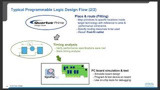
Timing Constraints and Optimization
Chapter 12 of 14
🔒 Unlock Audio Chapter
Sign up and enroll to access the full audio experience
Chapter Content
When designing complex systems, it’s crucial to consider timing constraints to ensure that all components function synchronously. This involves:
- Clock Domain Crossing: Managing data transfers between different clock domains (e.g., different frequencies or asynchronous signals).
- Timing Analysis: Use FPGA design tools to perform static timing analysis and identify potential timing violations.
- Resource Allocation: Optimize the placement of IP cores and custom logic to minimize signal propagation delays and reduce critical path lengths.
Detailed Explanation
Timing constraints ensure that all components of an FPGA design operate in sync, preventing errors. Managing clock domains and performing timing analysis are key to achieving this synchronization, while careful resource allocation reduces delays.
Examples & Analogies
Timing constraints are like scheduling a meeting across different time zones. You must consider the different available times (clock domains) and make sure everyone arrives (functions) at the same time without delays in communication.
Best Practices for System-Level FPGA Design
Chapter 13 of 14
🔒 Unlock Audio Chapter
Sign up and enroll to access the full audio experience
Chapter Content
Here are some best practices for successfully implementing system-level FPGA designs:
1. Plan the Design Architecture: Begin by clearly defining the overall system architecture, including the interaction between different subsystems and the IP cores. Use block diagrams to visualize the flow of data and control signals.
2. Use High-Level Design Abstraction: Start with high-level abstractions (e.g., using SystemVerilog or high-level synthesis tools) to quickly create prototypes and verify functionality before implementing low-level optimizations.
3. Leverage IP Cores: Use standard IP cores wherever possible to reduce development time. These cores have been tested and optimized for FPGA implementations.
4. Test Early and Often: Continuously simulate and test your design throughout the development process. Use modular testbenches and system-level simulations to validate each component before integration.
5. Optimize for Performance: After confirming functionality, focus on optimizing the design for performance by balancing resource usage, clock speeds, and timing constraints.
Detailed Explanation
These best practices provide a roadmap for effective FPGA design. They stress the importance of planning, utilizing high-level abstractions, and continuous testing. Implementing these strategies helps create robust and efficient systems.
Examples & Analogies
Think of best practices in FPGA design like best practices in cooking. Just as careful recipe planning, ingredient selection, and taste testing lead to a successful dish, following these design practices helps ensure a successful FPGA project.
Conclusion
Chapter 14 of 14
🔒 Unlock Audio Chapter
Sign up and enroll to access the full audio experience
Chapter Content
In this chapter, we explored the integration of IP cores and system-level design for FPGA-based systems. IP cores offer significant advantages in terms of design speed, reusability, and performance, and integrating them into a system requires a solid understanding of the FPGA’s architecture and design flow. System-level design practices ensure that these cores can be used efficiently and effectively to build complex, high-performance systems. By following the integration process and best practices outlined in this chapter, you can develop FPGA systems that meet your specific design requirements, offering flexibility and scalability for a wide range of applications.
Detailed Explanation
The chapter emphasizes the importance of IP cores in enhancing design efficiency and performance in FPGA systems. It highlights that understanding integration and system-level practices is crucial for developing versatile and robust designs.
Examples & Analogies
The conclusion connects everything by showing the broader impact of these design practices. Just as mastering a craft leads to high-quality outcomes, understanding and effectively integrating IP cores leads to superior FPGA designs.
Key Concepts
-
IP Cores: Pre-designed logic blocks essential for speeding up FPGA system designs.
-
Hard vs Soft IP Cores: Hard IP cores are fixed and high-performance while soft cores are flexible and HDL-defined.
-
System-Level Design: Integrates multiple components, optimizing their performance and interactions.
-
Modular Design: A strategy to build designs with reusable components for better maintainability.
-
Timing Optimization: Ensures all components function together without timing violations.
Examples & Applications
Using a DSP IP core for signal processing tasks in an audio application.
Implementing a UART IP core for serial communication between an FPGA and a microcontroller.
Memory Aids
Interactive tools to help you remember key concepts
Rhymes
IP picks are fast and neat, hard are fixed but soft can compete!
Stories
Imagine building a house with blocks. Hard blocks fit perfectly, but soft blocks allow you to change shape and size as needed.
Memory Tools
Remember HASS (Hard IP: Fast; Soft IP: Flexible) helps keep track of core types!
Acronyms
TIP - Timing, Integration, Performance
key aspects of system-level design.
Flash Cards
Glossary
- IP Core
A pre-designed reusable logic block or module that provides specific functionality in an FPGA design.
- Hard IP Core
A fixed hardware block implemented directly in the silicon of an FPGA, offering high performance.
- Soft IP Core
An IP core that can be described with HDL and synthesized into the FPGA's fabric, providing more flexibility.
- Communication Protocol
A set of rules governing data transmission between devices, essential for system integration.
- Modular Design
A method of structuring a system into smaller, manageable sub-modules, enhancing maintainability and reusability.
- System Bus
A communication pathway used to connect different IP cores and manage data transfers.
- Timing Constraints
Design requirements that ensure components within a system operate synchronously, preventing timing violations.
Reference links
Supplementary resources to enhance your learning experience.