
Timing Constraints and Optimization
Enroll to start learning
You’ve not yet enrolled in this course. Please enroll for free to listen to audio lessons, classroom podcasts and take practice test.
Interactive Audio Lesson
Listen to a student-teacher conversation explaining the topic in a relatable way.
Clock Domain Crossing
🔒 Unlock Audio Lesson
Sign up and enroll to listen to this audio lesson

Today, let's talk about Clock Domain Crossing. This is when we transfer data between two clock domains that might operate at different frequencies. Why do you think managing this is important?

Isn't it because if the clocks don't match, data can get lost or corrupted?
Exactly! That issue is known as metastability. It's crucial to design circuits that can handle this gracefully. One common technique to solve this is using synchronizers. Anyone heard of that?

Yeah, I think they help to synchronize signals from different clocks?
Correct! Remember: 'Synchronizers save signals!' — a good mnemonic to recall. By implementing such strategies, we ensure reliable data transfers!
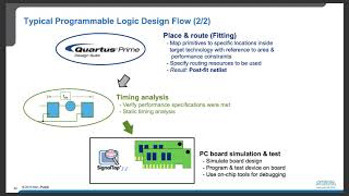
Timing Analysis
🔒 Unlock Audio Lesson
Sign up and enroll to listen to this audio lesson

Let’s delve into Timing Analysis. What tools do you think we can use to perform it?

I think tools like Vivado or Quartus can show timing violations?
That's right! These tools perform a static timing analysis, helping us identify where our design might fail to meet timing constraints. Why do you think this is crucial?

If we don’t check timing, the system might not work as expected, right?
Exactly. Meeting all timing requirements is crucial for system reliability. Remember: 'Timing matters, or your design shatters!'
Resource Allocation
🔒 Unlock Audio Lesson
Sign up and enroll to listen to this audio lesson
Next, let's talk about Resource Allocation. How does optimizing placement affect our design?
I think if we place components correctly, we can reduce delays?
Exactly! Proper placement minimizes signal propagation delays and can significantly reduce the critical path length. Can anyone remind us what the critical path is?
It's the longest path that data has to travel through the circuit, right?
That's correct! To remember this, think of 'Place and save the pace!' — effective placement keeps things moving without delays!
Introduction & Overview
Read summaries of the section's main ideas at different levels of detail.
Quick Overview
Standard
Timing constraints are crucial in FPGA designs to guarantee that all system components operate in unison. This section highlights techniques for managing clock domain crossings, conducting timing analysis, and optimizing resource allocation to minimize delays.
Detailed
Timing Constraints and Optimization
When designing complex systems using FPGAs, addressing timing constraints is essential to ensure all components function synchronously. This section elaborates on several important points regarding timing constraints and the optimization process:
- Clock Domain Crossing: This involves managing data transfers between different clock domains, which may include signals operating at different frequencies or asynchronous signals. Proper management helps avoid issues like metastability and ensures reliable data transfer.
- Timing Analysis: Conducting a static timing analysis using FPGA design tools allows designers to identify potential timing violations. This is crucial for assessing whether the timing requirements of the design are met.
- Resource Allocation: Optimizing how IP cores and custom logic are placed within the FPGA can significantly affect performance. Proper placement minimizes signal propagation delays and reduces critical path lengths, leading to a more efficient design.
By following these methods, designers can enhance the reliability and performance of FPGA-based systems, ultimately contributing to the successful integration of various components and features within the designs.
Youtube Videos


Audio Book
Dive deep into the subject with an immersive audiobook experience.
Clock Domain Crossing
Chapter 1 of 3
🔒 Unlock Audio Chapter
Sign up and enroll to access the full audio experience
Chapter Content
● Clock Domain Crossing: Managing data transfers between different clock domains (e.g., different frequencies or asynchronous signals).
Detailed Explanation
Clock domain crossing refers to the process of managing signals that move between different parts of a digital system that operate on different clock frequencies. When two components are clocked by different signals, there is a risk that data could be read by the receiving component at the wrong time, causing incorrect operations. To handle this, design strategies such as synchronization circuits or dual-clock FIFO buffers are used to ensure safe and reliable data transfer.
Examples & Analogies
Imagine a relay race where runners pass the baton to each other. If the first runner runs at a fast pace and passes the baton to a slower runner without careful timing, the second runner might not be ready to grab it, leading to a dropped baton. Similarly, in a digital design, if data is not transferred at the right moment between circuits that operate at different clock speeds, it can cause errors.
Timing Analysis
Chapter 2 of 3
🔒 Unlock Audio Chapter
Sign up and enroll to access the full audio experience
Chapter Content
● Timing Analysis: Use FPGA design tools to perform static timing analysis and identify potential timing violations.
Detailed Explanation
Timing analysis involves examining the timing characteristics of a digital system to ensure that all operations occur within the required time limits. This analysis helps to identify 'timing violations,' which occur when signals do not arrive at their destination in the expected time frame. FPGA design tools can perform static timing analysis, which checks the timing paths in a design without requiring dynamic simulation, allowing designers to optimize their circuits to meet the necessary clock constraints.
Examples & Analogies
Consider a train schedule where each train must reach its station on time to ensure smooth operations. If one train is delayed, it can cause a domino effect on the entire schedule. In design, if one signal path is too slow, it can delay the entire system's operation, hence the need for timing analysis to avoid such 'delays' in data processing.
Resource Allocation
Chapter 3 of 3
🔒 Unlock Audio Chapter
Sign up and enroll to access the full audio experience
Chapter Content
● Resource Allocation: Optimize the placement of IP cores and custom logic to minimize signal propagation delays and reduce critical path lengths.
Detailed Explanation
Resource allocation involves strategically placing various components of a digital design (like IP cores and custom logic) on the FPGA to improve performance. By minimizing the distances signals must travel (signal propagation delays) and shortening the critical path (the longest delay path through the circuit), designers can achieve faster operation speeds. This optimization is crucial to ensure that all signals are processed in sync with the clock cycles.
Examples & Analogies
Think of organizing a busy kitchen where chefs need to move between stations to prepare a meal. If the ingredients are too far apart, it takes longer to make the dish, causing delays. By placing ingredients and tools closer together, chefs can work more efficiently. Similarly, in FPGA design, optimizing the layout of components can speed up data processing.
Key Concepts
-
Clock Domain Crossing: Managing data flow between different clock frequencies to prevent data corruption.
-
Metastability: A state in digital circuits that can lead to signal errors if not properly managed.
-
Timing Analysis: Techniques used to ensure circuit signals meet timing requirements.
-
Critical Path: The longest delay path in a circuit design that determines the maximum operating speed.
-
Resource Allocation: Optimizing the placement of elements in an FPGA to reduce delays and improve performance.
Examples & Applications
Implementing a synchronizer for safe data transfer between two clock domains.
Using static timing analysis in Vivado to identify and rectify timing violations.
Memory Aids
Interactive tools to help you remember key concepts
Rhymes
If clocks collide, delays abide!
Stories
Imagine a train station where two trains arrive at different times; if the schedule is not managed well, chaos ensues. Just like in FPGA designs, managing clocks is critical.
Memory Tools
CLOCS: Clock management, Logic placement, Optimizing delays, Critical paths, Synchronization.
Acronyms
CROSS
Clock Reliability
Resource optimization
Overcoming signal conflicts.
Flash Cards
Glossary
- Clock Domain Crossing
The transfer of data between two different clock domains, which may operate at different frequencies.
- Metastability
A condition where a signal in a digital circuit can be in an indeterminate state, leading to unpredictable behavior.
- Timing Analysis
A process used to determine whether signals in a digital circuit meet predefined timing requirements.
- Critical Path
The longest sequence of operations in a digital circuit which determines the shortest time in which the circuit can operate.
- Resource Allocation
The process of placing IP cores and logical elements in an FPGA to optimize performance and minimize delays.
Reference links
Supplementary resources to enhance your learning experience.