
Conclusion
Interactive Audio Lesson
Listen to a student-teacher conversation explaining the topic in a relatable way.
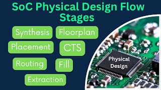
Importance of Physical Design Verification
🔒 Unlock Audio Lesson
Sign up and enroll to listen to this audio lesson

Today, we will discuss the importance of physical design verification. Why do you think it's critical in the VLSI design process?

I think it prevents errors that could come up during manufacturing.
Exactly! It ensures that our designs adhere to specifications. Without verification, we could face costly mistakes.

What kind of errors might happen if we skip this step?
Good question, Student_2! Errors can include incorrect chip functionality and issues with manufacturability, which we want to avoid at all costs.
Remember: Think of physical design verification as a safety net for our designs.

So it's like making sure everything fits together before we build it?
Exactly! Summarizing, physical design verification is essential to prevent manufacturing errors and costly design failures.
Methods for Physical Design Verification
🔒 Unlock Audio Lesson
Sign up and enroll to listen to this audio lesson

Let's explore the various methods used for physical design verification. What methods can you recall from our earlier discussions?
I remember Design Rule Checking (DRC) and Layout Versus Schematic (LVS).
Correct! DRC ensures layout compliance with manufacturing rules, while LVS checks if the physical layout matches the schematic. Anyone knows about Electrical Rule Checking (ERC)?

ERC checks the electrical behavior, right?
Spot on! ERC checks for signal integrity and electrical correctness. Don't forget about timing verification too, which is crucial for timing constraints.
How do these methods prevent issues?
Each method targets a specific type of verification, ensuring a comprehensive check of the design before moving to fabrication. In summary, using these methods helps us avoid functional errors and improves the reliability of the chip.
The Tape-Out Process
🔒 Unlock Audio Lesson
Sign up and enroll to listen to this audio lesson
Let’s discuss the tape-out process, which marks the end of the design phase. Why is tape-out significant?
Isn't it when we finalize the chip design for production?
Exactly! Tape-out involves generating the final GDSII files needed for fabrication. What are some preparations needed for tape-out, Student_1?
We need to ensure final DRC, LVS, and ERC checks are done?
Yes! We also need to verify timing and signal integrity before generating those files. What could happen if we rush this stage?
We might have mistakes that lead to manufacturing errors.
Exactly! Finalizing all checks is crucial to avoid delays and costly reworks. In summary, thorough verification during the tape-out process is vital for a successful transition from design to fabrication.
Introduction & Overview
Read summaries of the section's main ideas at different levels of detail.
Quick Overview
Standard
This section emphasizes the importance of physical design verification in the VLSI design process. It summarizes the methods used to guarantee that designs adhere to specifications and discusses the critical role of the tape-out process in transitioning the design from conception to fabrication.
Detailed
In VLSI design, physical design verification serves as a critical quality assurance process that ensures the correctness of the chip’s layout relative to design specifications and manufacturing rules. Key verification methods discussed include Design Rule Checking (DRC), Layout Versus Schematic (LVS), Electrical Rule Checking (ERC), and timing verification. The tape-out process represents the final phase of design before fabrication, requiring thorough final verifications to prevent manufacturing errors and ensure the chip's performance. Utilizing advanced Electronic Design Automation (EDA) tools, designers can achieve efficient, robust, and reliable chip designs ready for production.
Youtube Videos


Audio Book
Dive deep into the subject with an immersive audiobook experience.
Importance of Physical Design Verification
Chapter 1 of 4
🔒 Unlock Audio Chapter
Sign up and enroll to access the full audio experience
Chapter Content
Physical design verification is a vital step in ensuring that VLSI designs are manufacturable and function as expected.
Detailed Explanation
Physical design verification is essential in the VLSI design process. It ensures that the designed layout of the integrated circuit will work correctly and can be manufactured without issues. This step detects any potential errors or discrepancies before the design goes into production, thereby avoiding costly mistakes.
Examples & Analogies
Think of physical design verification like proofreading a manuscript before it gets published. Just as a proofreader checks for grammar errors and ensures everything is in order, physical design verification checks for errors in the chip layout to guarantee that the final product is correct and functional.
Methods of Physical Design Verification
Chapter 2 of 4
🔒 Unlock Audio Chapter
Sign up and enroll to access the full audio experience
Chapter Content
Through methods like Design Rule Checking (DRC), Layout Versus Schematic (LVS), Electrical Rule Checking (ERC), and timing verification, designers can ensure that their designs are free from errors.
Detailed Explanation
There are several methods employed in physical design verification to guarantee the integrity and functionality of the VLSI designs. Design Rule Checking (DRC) verifies that the layout complies with manufacturing rules. Layout Versus Schematic (LVS) checks that the physical layout matches the intended logical schematic. Electrical Rule Checking (ERC) focuses on the electrical behavior of the circuit. Timing verification ensures that all timing constraints are met.
Examples & Analogies
Imagine a classroom where students need to submit their homework assignments. The teacher checks for different things: the assignment must be legible (like DRC checks the physical layout), it must follow the required format (similar to LVS compliance), it must be on time (akin to timing verification), and it must not contain misleading information (like ERC checking electrical integrity).
Transition from Design to Fabrication
Chapter 3 of 4
🔒 Unlock Audio Chapter
Sign up and enroll to access the full audio experience
Chapter Content
The tape-out process marks the transition from design to fabrication, and it is crucial that all final verifications are completed to avoid costly errors during manufacturing.
Detailed Explanation
Tape-out is the final step in the design process, where the completed design is prepared for manufacturing. This stage is critical because it represents the moment when the design is committed to production. If any errors are found at this stage, it could lead to expensive fixes or even complete redesigns.
Examples & Analogies
Think of tape-out like booking a flight. Once you confirm the booking and pay, you can’t make any last-minute changes without facing penalties. In VLSI design, once the tape-out happens, it's a commitment to manufacture the chip, so ensuring everything is verified is paramount.
Using EDA Tools for Verification
Chapter 4 of 4
🔒 Unlock Audio Chapter
Sign up and enroll to access the full audio experience
Chapter Content
By using advanced EDA tools for verification and optimization, VLSI designers can achieve robust, efficient, and reliable chip designs ready for production.
Detailed Explanation
Electronic Design Automation (EDA) tools play a vital role in the verification process. These tools automate many checks to ensure designs comply with all standards and specifications, significantly reducing potential human errors and streamlining the process. By employing these tools, designers can optimize layouts and enhance efficiency.
Examples & Analogies
Consider EDA tools like power tools in a workshop. Just as power tools help a carpenter work more efficiently and accurately, EDA tools provide designers with capabilities to swiftly handle complex tasks, ensuring the design is perfect before construction starts.
Key Concepts
-
Physical Design Verification: Essential for ensuring manufacturable and functional VLSI designs.
-
DRC: Checks adherence to manufacturing rules to prevent defects.
-
LVS: Ensures layout matches the schematic to avoid functional errors.
-
ERC: Verifies electrical behaviors like signal integrity.
-
Tape-Out: Final validation step before moving to fabrication.
Examples & Applications
An engineer uses DRC tools to flag any violations in chip design, ensuring proper spacing between metal layers.
LVS is utilized to compare the schematic of a circuit to its physical layout, ensuring all connections are correct and in accordance with the design.
Memory Aids
Interactive tools to help you remember key concepts
Rhymes
DRC, LVS, and ERC show, a well-checked design will surely grow.
Stories
Imagine a builder checking every brick and beam before constructing a house. Similarly, engineers check every design aspect before tape-out to avoid future issues.
Memory Tools
Remember: 'DLETT' for Design - Layout - Electrical - Timing - Tape-out to recall key verification steps.
Acronyms
DRC
Defects Removed
Chips!
Flash Cards
Glossary
- Design Rule Checking (DRC)
A verification process that ensures the layout of a chip adheres to manufacturing rules specified by the semiconductor foundry.
- Layout Versus Schematic (LVS)
A verification step that ensures the physical layout of the circuit matches the intended logical schematic.
- Electrical Rule Checking (ERC)
Ensures that the electrical behavior of the design conforms to specified requirements.
- Timing Analysis Verification
Ensures that the layout meets required timing constraints, including setup and hold times.
- TapeOut
The final step in the VLSI design process before sending the chip design to the foundry for fabrication.
Reference links
Supplementary resources to enhance your learning experience.