
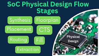
Preparation for Tape-Out
Interactive Audio Lesson
Listen to a student-teacher conversation explaining the topic in a relatable way.
Final Checks Before Tape-Out
🔒 Unlock Audio Lesson
Sign up and enroll to listen to this audio lesson

Before tape-out, we must ensure thorough verification of the design. Can anyone tell me what DRC stands for?

Design Rule Checking!
That's correct! DRC ensures that the layout adheres to manufacturing rules. What do we need to do if there are violations?

We have to fix those violations before proceeding.
Right! It's crucial to address any DRC, LVS, or ERC violations. Can someone explain what LVS is?

Layout Versus Schematic. It checks if the layout matches the schematic.
Exactly! We want to ensure connectivity in the layout is correct. Great job, everyone! Let’s summarize: final checks like DRC, LVS, and ERC prevent costly errors before tape-out.
Sign-Off Verification and GDSII Generation
🔒 Unlock Audio Lesson
Sign up and enroll to listen to this audio lesson

After all checks, what is the next step?

Sign-off verification?
Yes! This includes timing checks as well as power analysis. Why is this phase so important?
It ensures the chip operates correctly under real-world conditions!
Exactly! We need to confirm that our chip meets expectations. After this, we generate the GDSII file. Can anyone explain why GDSII is important?
It's the standard format for representing chip layouts and is used in fabrication.
Wonderful! To recap: sign-off verification ensures performance, and GDSII is crucial for fabrication.
Design Handoff to Foundry
🔒 Unlock Audio Lesson
Sign up and enroll to listen to this audio lesson
Once we've generated the GDSII files, what comes next?
The design is sent to the semiconductor foundry.
Correct! What additional checks does the foundry perform?
They ensure the design can be successfully fabricated.
Exactly! The foundry conducts manufacturing checks. Why are these checks necessary?
To avoid any errors during the chip manufacturing process!
Well said! Final checks by the foundry are crucial in preventing costly mistakes downstream. Remember, preparation for tape-out is key!
Introduction & Overview
Read summaries of the section's main ideas at different levels of detail.
Quick Overview
Standard
Before a chip design is sent for fabrication, it undergoes a series of final checks including DRC, LVS, and ERC to ensure compliance with design specifications. This stage culminates in GDSII file generation and design handoff to the semiconductor foundry.
Detailed
In the preparation for tape-out, several critical steps must be taken to ensure that the chip design is ready for fabrication. The process begins with a comprehensive set of final checks—Design Rule Checking (DRC), Layout Versus Schematic (LVS), and Electrical Rule Checking (ERC)—to ensure that no violations remain. Sign-off verification includes timing checks, power analysis, and signal integrity checks. Once these are completed, the final design data is converted into the GDSII format, an industry-standard for representing integrated circuit layouts. This GDSII file, along with the verified design, is handed off to the semiconductor foundry, which will then commence fabrication.
Youtube Videos


Audio Book
Dive deep into the subject with an immersive audiobook experience.
Final DRC, LVS, and ERC Checks
Chapter 1 of 4
🔒 Unlock Audio Chapter
Sign up and enroll to access the full audio experience
Chapter Content
Before tape-out, the following steps must be completed:
- Final DRC, LVS, and ERC Checks: A final round of physical design verification must be performed to ensure that no violations exist. Any remaining DRC, LVS, or ERC violations must be fixed before the design can be taped-out.
Detailed Explanation
Before the tape-out process can begin, the design undergoes final verification checks. This step involves executing Design Rule Checking (DRC), Layout Versus Schematic (LVS), and Electrical Rule Checking (ERC). Each of these checks ensures that the design adheres to the required manufacturing specifications and that any errors are corrected. If there are any violations from these checks, they must be resolved; otherwise, the design cannot be sent for fabrication.
Examples & Analogies
Think of this step like a thorough pre-flight checklist that pilots complete before taking off. Just as pilots check the aircraft's systems to make sure everything is functioning correctly before leaving the ground, engineers check their designs to ensure that there are no errors before sending it off to be manufactured. Both processes are critical for safety and success.
Sign-Off Verification
Chapter 2 of 4
🔒 Unlock Audio Chapter
Sign up and enroll to access the full audio experience
Chapter Content
- Sign-Off Verification: The design undergoes final verification, including timing checks (STA), power analysis, and signal integrity checks to ensure that the chip will operate as expected under real-world conditions.
Detailed Explanation
After the initial verification checks, the next step is Sign-Off Verification. This involves conducting additional checks like Static Timing Analysis (STA), power analysis, and signal integrity checks. The purpose is to ensure that the chip will function correctly in practice, accounting for real-world conditions it will face once fabricated. This comprehensive verification process enhances the reliability of the design.
Examples & Analogies
You can liken Sign-Off Verification to a car inspection before a long road trip. Just as a mechanic checks the brakes, lights, and engine to ensure the car will perform well on the road, engineers perform final checks on the chip design to make sure everything works efficiently and reliably once it's built.
GDSII File Generation
Chapter 3 of 4
🔒 Unlock Audio Chapter
Sign up and enroll to access the full audio experience
Chapter Content
- GDSII File Generation: The final design data is converted into the GDSII format, which is the industry standard for representing the layout of integrated circuits. This file contains all the information required for fabrication, including layer definitions and geometry.
Detailed Explanation
Once all tests and checks are complete, the design data is converted into a GDSII file. This file format is crucial as it encapsulates all the necessary details about the chip's physical layout, including its geometry, layers, and features. This standardization simplifies the interfacing between design teams and fabrication plants, ensuring that all necessary information is accessible and clear for manufacturing.
Examples & Analogies
Consider the GDSII file generation as preparing a blueprint for a building. Just like architects provide detailed plans and diagrams to the construction team, engineers create GDSII files to ensure that the foundry has all the information needed to fabricate the chip accurately and efficiently.
Design Handoff to Foundry
Chapter 4 of 4
🔒 Unlock Audio Chapter
Sign up and enroll to access the full audio experience
Chapter Content
- Design Handoff to Foundry: Once the GDSII files are generated, they are sent to the semiconductor foundry, where they will be used to fabricate the chip. The foundry performs additional manufacturing checks to ensure the design can be fabricated successfully.
Detailed Explanation
The final step in preparation before tape-out is handing over the GDSII files to the semiconductor foundry. At this stage, the foundry will utilize these files to begin the fabrication process of the chip. Additionally, the foundry will conduct its own checks to verify that the design can indeed be produced based on its specifications and the manufacturing capabilities.
Examples & Analogies
Imagine sending a recipe to a bakery for them to bake a cake. Once you hand over the carefully written recipe—which includes ingredients and instructions—the bakery confirms that they have what they need to create the cake successfully. Similarly, in chip design, handing off the GDSII files is like providing the foundry with the perfect recipe for creating the chip.
Key Concepts
-
Final Checks: DRC, LVS, and ERC prevent errors before tape-out.
-
Sign-Off Verification: Ensures the design operates as expected.
-
GDSII Generation: Standard format for chip fabrication.
-
Design Handoff: The transfer of verified design to the semiconductor foundry.
Examples & Applications
Example 1: If a DRC violation occurs due to insufficient spacing, the layout must be adjusted before tape-out.
Example 2: LVS helps verify that every connection in the schematic proper reflects in the layout.
Memory Aids
Interactive tools to help you remember key concepts
Rhymes
Before the tape-out, check the layout, DRC, LVS - keep errors out!
Stories
Imagine a builder needing to verify blueprints against the constructed house; this ensures everything is in place just like LVS compares the layout to the schematic.
Memory Tools
Remember 'D-L-E' to recall DRC, LVS, and ERC for design checks—Design, Layout, Electrical.
Acronyms
DRC for Design Rules, LVS for Layout Validation, ERC for Electrical Compliance - remember DLE for preparation steps.
Flash Cards
Glossary
- DRC (Design Rule Checking)
A verification method that ensures chip layout adheres to manufacturing rules.
- LVS (Layout Versus Schematic)
A process verifying that the physical layout matches the logical schematic design.
- ERC (Electrical Rule Checking)
A verification method ensuring electrical behavior meets specified design constraints.
- GDSII
A file format used to represent the physical layout of integrated circuits.
- SignOff Verification
Final checks to ensure the design meets specifications before fabrication.
Reference links
Supplementary resources to enhance your learning experience.