
Methods for Physical Design Verification
Interactive Audio Lesson
Listen to a student-teacher conversation explaining the topic in a relatable way.
Design Rule Checking (DRC)
🔒 Unlock Audio Lesson
Sign up and enroll to listen to this audio lesson

Today, we are going to explore Design Rule Checking, commonly referred to as DRC. This method ensures that our chip layouts follow the manufacturing rules set by the semiconductor foundries.

What kind of rules are we talking about?
Great question! DRC checks for design constraints like minimum spacing and widths of features such as transistors and metal layers. If any aspect fails to meet these rules, we have a DRC violation.

Can you give an example of a DRC violation?
Sure! For instance, if metal traces are too close together, it could lead to short circuits. Automating DRC checks with tools like Cadence Calibre helps us catch these issues quickly.

What tools do we use for these checks?
We mainly use specialized EDA tools. Cadence Calibre, Mentor Graphics PADS, and Synopsys IC Validator are very common. Remember: DRC = Design Rule Compliance!
To recap, DRC is crucial for avoiding manufacturing defects by ensuring adherence to specified design rules.
Layout Versus Schematic (LVS)
🔒 Unlock Audio Lesson
Sign up and enroll to listen to this audio lesson

Next, let's move on to Layout Versus Schematic, abbreviated as LVS. This step verifies that our physical layout matches the logical schematic.

What happens if there is a discrepancy?
If mismatches occur, it can lead to functional errors, like incorrect component connections. LVS helps highlight these issues before manufacturing.
Which tools do we use for LVS?
We typically use tools such as Cadence Virtuoso or Mentor Graphics Calibre. They compare the layout to the schematic netlist and report any inconsistencies.
So, it's important that LVS ensures our design follows the intended logical paths. Any questions?
Can LVS handle large designs?
Absolutely! LVS tools are designed to manage complex designs efficiently, ensuring accuracy in larger projects.
In summary, LVS is vital for matching our physical layout with the schematic, preventing logical errors.
Electrical Rule Checking (ERC)
🔒 Unlock Audio Lesson
Sign up and enroll to listen to this audio lesson
Now we will discuss Electrical Rule Checking or ERC. ERC assesses the electrical behavior of our designs against defined requirements.
What are some common violations we might find?
Common violations include floating nodes, insufficient drive strength, or incorrect power connections. These can significantly affect chip functionality.
How do we perform these checks?
Similar to DRC and LVS, we use EDA tools like Cadence Virtuoso and Mentor Graphics Calibre, which analyze the layout for electrical integrity.
Remember: ERC = Electrical Behavior Compliance! It ensures our design’s electrical characteristics meet specifications.
To sum up, ERC checks for electrical issues that could cause reliability failures in the final chip.
Timing Analysis Verification
🔒 Unlock Audio Lesson
Sign up and enroll to listen to this audio lesson
Let’s discuss Timing Analysis Verification, which focuses on timing constraints such as setup and hold times using Static Timing Analysis, or STA.
What kind of violations can occur in timing analysis?
Timing violations can happen when delays along critical paths exceed allowable limits. This could lead to incorrect data being latched by flip-flops.
What tools assist with timing verification?
Tools like Synopsys PrimeTime and Cadence Tempus are very effective in performing these timing analyses.
Overall, timing analysis is crucial for ensuring our design meets performance specifications, especially with high-speed operations!
In conclusion, timing verification is key to obtaining optimal performance and preventing data errors.
Signal Integrity Checking
🔒 Unlock Audio Lesson
Sign up and enroll to listen to this audio lesson
Finally, we will cover Signal Integrity Checking. This is crucial for designs operating at high speeds, ensuring signals do not degrade due to interference.
What types of issues does signal integrity check for?
Signal integrity checks look for problems like crosstalk and excessive noise. These can significantly lead to functional errors.
Which tools do we use for this type of analysis?
We typically use tools like Cadence Sigrity or Mentor Graphics HyperLynx to analyze layouts for signal interference.
To summarize, signal integrity helps maintain quality in our high-speed designs by identifying potential interference early.
Introduction & Overview
Read summaries of the section's main ideas at different levels of detail.
Quick Overview
Standard
In this section, we delve into various methods of physical design verification essential for ensuring that semiconductor chip layouts meet design specifications and manufacturing rules. Major methods discussed include DRC, LVS, ERC, Timing Analysis, and Signal Integrity Checking, each critical for mitigating risks associated with manufacturing defects.
Detailed
Methods for Physical Design Verification
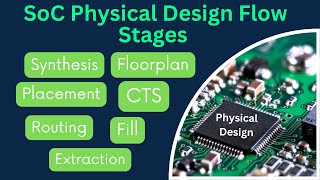
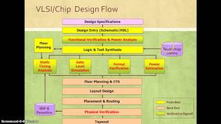
Physical design verification is an essential step within the VLSI design process that ensures physical layouts conform to necessary specifications and manufacturing rules. The key methods for physical design verification include:
1. Design Rule Checking (DRC)
- Definition: DRC ensures that the layout adheres to manufacturing rules from the semiconductor foundry, including minimum spacing and width for features.
- Violations: Errors that violate design rules, leading to potential manufacturing defects.
- Tools: Specialized EDA tools are used for automated checks (e.g., Cadence Calibre, Mentor Graphics PADS).
2. Layout Versus Schematic (LVS)
- Definition: LVS validates that the physical layout matches the intended schematic, ensuring proper connectivity.
- Violations: Discrepancies lead to functional errors.
- Tools: Tools like Cadence Virtuoso are utilized for this verification.
3. Electrical Rule Checking (ERC)
- Definition: ERC checks for the electrical behavior of the design against specified requirements.
- Violations: Includes floating nodes and incorrect connections leading to reliability issues.
- Tools: Similar EDA tools for ERC as used in DRC and LVS.
4. Timing Analysis Verification
- Definition: Ensures timing constraints are met, such as setup and hold times using Static Timing Analysis (STA).
- Violations: Timing violations occur when path delays exceed allowable limits.
- Tools: Tools like Synopsys PrimeTime perform reliable timing analysis.
5. Signal Integrity Checking
- Definition: Ensures that signal quality is maintained in high-speed designs, avoiding issues like crosstalk.
- Tools: Tools such as Cadence Sigrity are employed for this type of analysis.
In summary, these methods are pivotal for identifying and correcting design errors early, thereby ensuring successful chip fabrication.
Youtube Videos

Audio Book
Dive deep into the subject with an immersive audiobook experience.
Overview of Physical Design Verification
Chapter 1 of 6
🔒 Unlock Audio Chapter
Sign up and enroll to access the full audio experience
Chapter Content
Physical design verification ensures that the physical layout of the design conforms to the required specifications and rules.
Detailed Explanation
Physical design verification is a crucial part of the design process for silicon chips. This step checks whether the physical design – the arrangement of components like transistors and wires on the chip – meets all the necessary specifications outlined by the design engineer and the manufacturing rules of the semiconductor foundry. It is vital to perform these verifications to avoid errors that could cause the chips to malfunction after they are manufactured.
Examples & Analogies
Imagine you are building a puzzle. Before you finish, you need to ensure that every piece fits perfectly according to the picture on the box. If one piece doesn’t fit, the completed puzzle won’t look right. Similarly, physical design verification ensures that every element of the chip design fits together correctly, according to specifications.
Design Rule Checking (DRC)
Chapter 2 of 6
🔒 Unlock Audio Chapter
Sign up and enroll to access the full audio experience
Chapter Content
Design Rule Checking (DRC) is a process that ensures that the layout of the chip adheres to the manufacturing rules specified by the semiconductor foundry. These rules define the minimum allowable spacing, width, and other design constraints for features such as transistors, metal layers, and vias.
Detailed Explanation
DRC focuses on verifying that the layout follows the rules set by manufacturing standards. These rules are critical because they define how closely components can be placed to prevent issues during the manufacturing stage, such as short circuits or material failures. When the layout is checked against these rules, violations are flagged if any spacing is too narrow or if any component is outside the allowed dimensions.
Examples & Analogies
Think of DRC like building codes for construction. Just as buildings must adhere to certain codes regarding spacing and material types to ensure safety, chip designs must comply with manufacturing rules to ensure they can be produced without defects.
Layout Versus Schematic (LVS)
Chapter 3 of 6
🔒 Unlock Audio Chapter
Sign up and enroll to access the full audio experience
Chapter Content
Layout Versus Schematic (LVS) is a verification step that ensures that the physical layout of the circuit matches the intended logical schematic. LVS checks for discrepancies between the layout and the netlist, ensuring that the connectivity of components in the layout is consistent with the schematic design.
Detailed Explanation
LVS involves comparing the physical arrangement of components (the layout) to the planned design (the schematic). This is important because the layout must accurately reflect the electrical connections denoted in the schematic. If there are discrepancies, for example, a transistor is incorrectly connected, it could lead to failures in the circuit’s functionality.
Examples & Analogies
Imagine you are assembling a circuit board from a blueprint. If you place a resistor where a capacitor should be according to the blueprint, the board won’t work as intended. LVS ensures that what you’ve built matches the original design.
Electrical Rule Checking (ERC)
Chapter 4 of 6
🔒 Unlock Audio Chapter
Sign up and enroll to access the full audio experience
Chapter Content
Electrical Rule Checking (ERC) ensures that the electrical behavior of the design conforms to the specified requirements. ERC checks for issues like signal integrity, power integrity, and violation of electrical design constraints.
Detailed Explanation
ERC focuses on ensuring that the circuit's electrical performance meets necessary criteria. This includes checking for proper voltage levels, current pathways, and identifying potential issues such as floating nodes or incorrect power connections. Any violations found during ERC can have serious impacts on the reliability and functionality of the final chip.
Examples & Analogies
Consider ERC like ensuring the plumbing in a house works correctly. If pipes are connected improperly or leaks are present, the water supply will not function as needed. Similarly, ERC checks the ‘electrical plumbing’ of the chip to ensure everything flows properly.
Timing Analysis Verification
Chapter 5 of 6
🔒 Unlock Audio Chapter
Sign up and enroll to access the full audio experience
Chapter Content
Timing verification ensures that the layout meets the required timing constraints, including setup and hold times, clock skew, and propagation delay.
Detailed Explanation
Timing verification checks if signals within the chip arrive at their destinations within the required timeframes to ensure synchronization. If signals do not meet these timing constraints, it can lead to faults, such as data being latched incorrectly by flip-flops, which can cause the entire system to malfunction.
Examples & Analogies
Timing analysis is like ensuring synchronized timing in a relay race. All runners must pass the baton within a set time frame; otherwise, the team will incur penalties or lose the race. Similarly, signals must be timed correctly to ensure the chip functions as intended.
Signal Integrity Checking
Chapter 6 of 6
🔒 Unlock Audio Chapter
Sign up and enroll to access the full audio experience
Chapter Content
Signal integrity verification ensures that the signals in the design do not experience unwanted interference, such as crosstalk or excessive noise.
Detailed Explanation
Signal integrity verification checks to ensure that the electrical signals traversing the chip do not compromise performance due to interference like noise or crosstalk between adjacent signal lines. This is particularly important in high-speed circuits where even minor interference can result in significant errors.
Examples & Analogies
Think of signal integrity like a crowded public space where people are talking loudly. If the noise level is too high, it becomes hard to hear a single voice clearly. Similarly, crosstalk can muddle signals in a chip, leading to miscommunication.
Key Concepts
-
DRC: Ensures layout follows manufacturing rules.
-
LVS: Confirms layout matches schematic connectivity.
-
ERC: Validates electrical behavior meets design specifications.
-
Timing Analysis: Checks that timing constraints are satisfied.
-
Signal Integrity: Assures signal quality is maintained during transmission.
Examples & Applications
A DRC violation occurs if metal traces in the layout are too close, risking a short circuit.
An LVS violation could manifest if the layout has additional transistors not present in the schematic.
ERC might flag a floating node if a wiring connection is left incomplete, causing reliability issues.
Timing analysis checks if the signal delay on a data path exceeds the defined setup time, which can lead to malfunction.
Signal integrity issues could arise from two adjacent signal lines causing crosstalk during high-speed operation, degrading performance.
Memory Aids
Interactive tools to help you remember key concepts
Rhymes
For designs that won’t crack, check the DRC back!
Stories
Once upon a time in chip land, a layout tried to jump the manufacturing rules. The wise old DRC caught it before the job's end, saving many chips from ill fate!
Memory Tools
Remember D-R-E-T-S: DRC, LVS, ERC, Timing Analysis, Signal Integrity for all verification needs.
Acronyms
LVS = Layout Validates Schematic, an acronym to remember its purpose.
Flash Cards
Glossary
- Design Rule Checking (DRC)
A process to ensure that the layout adheres to the manufacturing rules specified by the semiconductor foundry.
- Layout Versus Schematic (LVS)
A verification step that checks if the physical layout of a circuit matches the intended schematic design.
- Electrical Rule Checking (ERC)
A process that verifies the electrical behavior of designs against specified requirements.
- Static Timing Analysis (STA)
A method used to validate timing constraints in digital circuits.
- Signal Integrity Checking
A verification process that ensures signal quality is maintained, especially in high-speed designs.
Reference links
Supplementary resources to enhance your learning experience.
- Design Rule Checking (DRC) Explained
- Layout versus Schematic (LVS) Verification
- Electrical Rule Checking (ERC) Overview
- Static Timing Analysis Using Synopsys PrimeTime
- Signal Integrity Analysis in VLSI
- Introduction to VLSI Design Flow
- VLSI Physical Design Verification Methods
- Signal Integrity Techniques in Modern Designs