
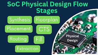
Physical Design Verification
Interactive Audio Lesson
Listen to a student-teacher conversation explaining the topic in a relatable way.
Introduction to Physical Design Verification
🔒 Unlock Audio Lesson
Sign up and enroll to listen to this audio lesson

Welcome everyone! Today we'll talk about physical design verification and why it's crucial in the VLSI design process. Can anyone tell me what they think physical design verification involves?

Is it about checking if the chip's design follows certain rules?
Exactly! Physical design verification ensures that the chip layout adheres to specifications to avoid manufacturing errors. It's all about compliance with design rules, timing, power, and manufacturability. Think of it as a final checkpoint before production!

What happens if the design doesn't meet these specifications?
Good question! If the design doesn’t comply, it can result in costly errors during manufacturing, leading to functional failures. That's why methods like DRC, LVS, and ERC are essential!

Can you give an example of a violation?
Sure! An example of a DRC violation could be insufficient spacing between metal traces, which could cause short circuits. Remember, proper layout is key!

So DRC is all about the layout rules, right?
That's correct! Let's move on to the specific methods employed for physical verification.
Design Rule Checking (DRC)
🔒 Unlock Audio Lesson
Sign up and enroll to listen to this audio lesson

Now, let's dive deeper into Design Rule Checking, commonly abbreviated as DRC. Can someone explain what DRC checks for?
It checks if the layout follows the manufacturing rules, right?
Exactly! DRC verifies that the chip layout meets the semiconductor foundry's manufacturing constraints. Tools like Cadence Calibre automate this process.
What happens if DRC finds a violation?
If a violation occurs, such as an improperly spaced feature, it can lead to signal integrity problems or even defects in manufacturing. Correcting these violations before proceeding is essential!
Are there other methods similar to DRC?
Yes, indeed! After DRC, we typically perform LVS to verify the layout against the schematic. Would anyone like to explain what LVS does?
Layout Versus Schematic (LVS)
🔒 Unlock Audio Lesson
Sign up and enroll to listen to this audio lesson
Let's discuss Layout Versus Schematic, or LVS for short. Who can explain the significance of LVS in the design process?
LVS makes sure that the physical layout matches the logical design, right?
Spot on! LVS verifies that each connection in the layout corresponds correctly to the schematic. If a transistor is misplaced, for instance, it can create functional errors in the circuit.
What tools can we use for LVS?
We generally use tools like Cadence Virtuoso for LVS checks. These tools compare the layout and the schematic netlist. Remember, ensuring consistency between layout and schematic is critical!
And what about ERC? How does that fit in?
Great segue! ERC, or Electrical Rule Checking, focuses on the electrical behavior of the design. Let's explore that next!
Electrical Rule Checking (ERC)
🔒 Unlock Audio Lesson
Sign up and enroll to listen to this audio lesson
Now that we've covered LVS, let's discuss ERC. What do we think ERC checks for?
I think it looks at the electrical characteristics of the layout, like power connections?
Exactly! ERC checks for issues such as insufficient drive strength or floating nodes that could compromise functionality. Tools like Synopsys IC Validator help with these checks.
Can we have a real-world example of an ERC violation?
Absolutely! An example would be an improper connection between the ground and power rail leading to reliability issues. These errors can cause functionality failures in the final chip.
So we need to catch ERC violations before tape-out?
Absolutely! Speaking of tape-out, let's move on to understanding that process and the challenges it entails.
The Tape-Out Process
🔒 Unlock Audio Lesson
Sign up and enroll to listen to this audio lesson
Now, we arrive at the tape-out process, the final step in the VLSI design cycle. Can anyone share what tape-out involves?
Is tape-out when the design is sent for fabrication?
That's correct! But before that, we must conduct final DRC, LVS, and ERC checks. Final verification is key, ensuring no violations exist!
What challenges might arise during tape-out?
Excellent question! Challenges can include last-minute design changes that require rework and ensuring timing closure. These must be addressed before final sign-off!
What does tape-out sign-off mean for the design team?
Tape-out sign-off signifies that the design team has approved the chip for fabrication, ensuring all documentation is final and the design is manufacturable. Remember, the role of verification in avoiding costly errors can't be overstated!
Thank you, that really clarifies the entire process!
You're welcome! To summarize, physical design verification involves various checks like DRC, LVS, and ERC, culminating in the tape-out process—a crucial transition from design to production.
Introduction & Overview
Read summaries of the section's main ideas at different levels of detail.
Quick Overview
Standard
This section delves into physical design verification methods including Design Rule Checking (DRC), Layout Versus Schematic (LVS), and Electrical Rule Checking (ERC). It highlights the significance of these checks in the VLSI design process and concludes with an overview of the tape-out process, ensuring readiness for chip fabrication.
Detailed
Physical Design Verification
Physical design verification is an essential step in the VLSI design process, aimed at ensuring that a chip's physical layout meets all design specifications and manufacturing rules. This motivated verification process plays a crucial role in preventing costly design errors during chocolate manufacturing of chips.
Key Methods of Physical Design Verification
-
Design Rule Checking (DRC): This method checks the layout against the semiconductor foundry’s manufacturing rules to flag violations (e.g., improper spacing).
- Tools: EDA tools such as Cadence Calibre help automate this process.
-
Layout Versus Schematic (LVS): LVS ensures that the physical layout corresponds with the logical schematic, identifying any connectivity discrepancies between the two.
- Tools: Commonly used tools include Cadence Virtuoso.
-
Electrical Rule Checking (ERC): This checks the electrical behavior of the design against specified requirements, focusing on issues such as signal integrity and power connections.
- Tools: ERC is often carried out using EDA tools like Synopsys IC Validator.
-
Timing Analysis Verification: It verifies that the layout meets timing constraints to ensure reliable functionality, employing static timing analysis.
- Tools: Often conducted with Synopsys PrimeTime.
-
Signal Integrity Checking: This step ensures that signals remain clear of unwanted interference, particularly in high-speed designs.
- Tools: Tools like Cadence Sigrity analyze crosstalk and noise levels in the layout.
Tape-Out Process Overview
Tape-out represents the transition from design to fabrication, necessitating the successful generation of GDSII files that encapsulate the physical layout. Key stages include:
- Final Verifications: A comprehensive check for DRC, LVS, and ERC violations.
- GDSII File Generation: Final layout data in the GDSII format is produced before sending it to the fabrication foundry.
- Challenges: Issues like last-minute design changes and timing closure must be addressed in final verifications.
Overall, physical design verification is vital in ensuring manufacturability and expected functionality of VLSI designs, helping to avoid errors that could arise during the production process.
Youtube Videos

Audio Book
Dive deep into the subject with an immersive audiobook experience.
Introduction to Physical Design Verification
Chapter 1 of 10
🔒 Unlock Audio Chapter
Sign up and enroll to access the full audio experience
Chapter Content
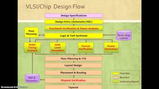
Physical design verification is a critical step in the VLSI design process that ensures that the physical layout of a chip adheres to the design specifications and manufacturing rules. Verification ensures that the chip will function correctly when fabricated, avoiding costly design errors that may arise during manufacturing. The primary objective of physical design verification is to check the correctness of the layout with respect to various constraints, such as design rules, timing, power, and manufacturability.
Detailed Explanation
In VLSI design, physical design verification is an essential step that confirms that the chip's layout matches both the design specifications and the rules set by manufacturers. This process prevents costly mistakes that could occur during actual production. The aim is to ensure that the chip will function correctly by checking various parameters like the distance between components (design rules), the time signals take to travel (timing), how much power the chip consumes, and its ease of manufacturing.
Examples & Analogies
Imagine building a house according to specific architectural blueprints. Before construction begins, an inspector checks that the plan is followed—like ensuring doors are at specified widths and windows are placed correctly. If these details are ignored, the house might have fundamental issues once built. Similarly, physical design verification checks a chip's layout against its design before it is manufactured.
Methods for Physical Design Verification
Chapter 2 of 10
🔒 Unlock Audio Chapter
Sign up and enroll to access the full audio experience
Chapter Content
Physical design verification ensures that the physical layout of the design conforms to the required specifications and rules. The key methods for physical design verification include Design Rule Checking (DRC), Layout Versus Schematic (LVS), and Electrical Rule Checking (ERC).
Detailed Explanation
There are various methods used for physical design verification: Design Rule Checking (DRC) verifies that the layout meets manufacturing rules, Layout Versus Schematic (LVS) ensures that the physical layout aligns with the schematic representation of the design, and Electrical Rule Checking (ERC) analyzes the design for electrical integrity.
Examples & Analogies
Think of these verification methods like a recipe check in cooking. DRC is like ensuring you have all the ingredients in the right quantities (like spacing on a chip), LVS is like making sure the dish looks like what you intended (sauce is on the pasta), and ERC is ensuring that the dish isn’t flawed in taste or texture (like avoiding over-salted food). Each check ensures the final dish, or in this case, a functional chip, turns out right.
Design Rule Checking (DRC)
Chapter 3 of 10
🔒 Unlock Audio Chapter
Sign up and enroll to access the full audio experience
Chapter Content
Design Rule Checking (DRC) is a process that ensures that the layout of the chip adheres to the manufacturing rules specified by the semiconductor foundry. These rules define the minimum allowable spacing, width, and other design constraints for features such as transistors, metal layers, and vias. DRC Violations: If a layout feature violates these design rules (e.g., insufficient spacing between metal traces or too narrow a wire), a DRC violation is flagged. These violations can lead to manufacturing defects, signal integrity problems, or reliability issues. Tools for DRC: DRC is typically performed using specialized EDA tools that automatically check the design against the manufacturing process rules. Tools like Cadence Calibre, Mentor Graphics PADS, and Synopsys IC Validator are widely used for DRC checks.
Detailed Explanation
DRC is vital because it ensures that the chip layout follows strict guidelines set by manufacturers, which include the minimum distance between features and their sizes. When a violation occurs, it can result in issues during production, such as faulty chips. Tools are utilized to automatically identify these violations, allowing designers to correct mistakes early in the design phase.
Examples & Analogies
Continuing with the house analogy, DRC is akin to ensuring that walls are the right thickness and are spaced correctly from each other, preventing future structural problems. If a wall is too thin or too close to another, it could eventually lead to the house collapsing or requiring costly repairs.
Layout Versus Schematic (LVS)
Chapter 4 of 10
🔒 Unlock Audio Chapter
Sign up and enroll to access the full audio experience
Chapter Content
Layout Versus Schematic (LVS) is a verification step that ensures that the physical layout of the circuit matches the intended logical schematic. LVS checks for discrepancies between the layout and the netlist, ensuring that the connectivity of components in the layout is consistent with the schematic design. LVS Violations: LVS violations occur if there are mismatches between the layout and the schematic. This can happen if, for example, the wrong transistor is placed or connected in the layout, leading to functional errors in the circuit. Tools for LVS: LVS is performed using tools like Cadence Virtuoso, Mentor Graphics Calibre, and Synopsys IC Validator that compare the layout and the schematic netlist and generate reports highlighting discrepancies.
Detailed Explanation
LVS ensures that the layout physically represents what the designer intended in the schematic. If there's a mistake in how components are connected or if the wrong components are used, it can lead to failures in the actual circuit. By using automated tools, designers can easily identify and correct these discrepancies, ensuring that the design will function as expected once fabricated.
Examples & Analogies
Think of LVS like checking a map against a GPS system. If the GPS shows a different route than the map illustrates, there lies a problem. Similarly, LVS checks that the layout is a true representation of the intended circuit design before proceeding with manufacturing.
Electrical Rule Checking (ERC)
Chapter 5 of 10
🔒 Unlock Audio Chapter
Sign up and enroll to access the full audio experience
Chapter Content
Electrical Rule Checking (ERC) ensures that the electrical behavior of the design conforms to the specified requirements. ERC checks for issues like signal integrity, power integrity, and violation of electrical design constraints. Common ERC violations include issues like floating nodes, insufficient drive strength, and incorrect power or ground connections. These errors can lead to functionality failures or reliability issues in the final chip. Tools for ERC: ERC checks are typically performed using EDA tools that analyze electrical connections within the layout. Cadence Virtuoso, Mentor Graphics Calibre, and Synopsys IC Validator also provide ERC capabilities.
Detailed Explanation
ERC aims to ensure that the way electrical signals behave in the design meets the required standards. It checks for potential issues that could cause the final chip to malfunction, such as signals that aren't strong enough or incorrect power connections. By using EDA tools, designers can automate this checking process, simplifying identifying electrical issues.
Examples & Analogies
Imagine a plumbing system in a house. If the pipes aren't connected correctly (missing water flow), or if they aren't strong enough to handle water pressure, leaks could occur. Similarly, ERC ensures that all electrical elements are correctly connected and functioning to prevent failures.
Timing Analysis Verification
Chapter 6 of 10
🔒 Unlock Audio Chapter
Sign up and enroll to access the full audio experience
Chapter Content
Timing verification ensures that the layout meets the required timing constraints, including setup and hold times, clock skew, and propagation delay. This process typically involves static timing analysis (STA), which checks the timing of all signal paths in the design, from registers to combinational logic. Timing Violations: Timing violations occur when the delay along a critical path exceeds the allowable time, leading to setup or hold violations, which could cause incorrect data to be latched by flip-flops. Tools for Timing Verification: Tools like Synopsys PrimeTime and Cadence Tempus are widely used for timing analysis, checking the timing constraints of the design and ensuring that they are met after placement and routing.
Detailed Explanation
In timing verification, the goal is to ensure that signals arrive at the correct time and that all timing requirements are satisfied. If there is any delay beyond acceptable limits, data can be incorrectly processed, leading to errors in chip behavior. Tools are used to perform these analyses systematically, identifying any potential timing problems before fabrication.
Examples & Analogies
Think of timing analysis like a relay race. Each runner (signal) must reach their designated point on time for the baton (data) to be passed effectively. If one runner is late (timing violation), it can disrupt the entire race, similar to how timing violations can affect digital circuits.
Signal Integrity Checking
Chapter 7 of 10
🔒 Unlock Audio Chapter
Sign up and enroll to access the full audio experience
Chapter Content
Signal integrity verification ensures that the signals in the design do not experience unwanted interference, such as crosstalk or excessive noise. This is especially important in high-speed designs where signal degradation can lead to functional errors. Crosstalk Analysis: This type of analysis identifies signal lines that are too close together, potentially causing interference between them, leading to crosstalk. Tools for Signal Integrity: Signal integrity tools like Cadence Sigrity and Mentor Graphics HyperLynx are used to perform checks on the layout for potential issues like crosstalk, power noise, and other signal interference.
Detailed Explanation
Signal integrity checking is essential, particularly for designs that operate at high speeds, as interference can disrupt signals and cause errors. Crosstalk is a common problem, where signals from one line can unintentionally affect another. Using specialized tools, designers can analyze and mitigate such issues to ensure reliable performance.
Examples & Analogies
Imagine a crowded room where people are trying to talk (signals). If everyone speaks loudly and is too close together (crosstalk), it becomes difficult to hear properly (signal disruption). Signal integrity checks help ensure that conversations can happen clearly without interference.
Overview of the Tape-Out Process
Chapter 8 of 10
🔒 Unlock Audio Chapter
Sign up and enroll to access the full audio experience
Chapter Content
Tape-out is the final step in the VLSI design process before the chip is sent to the semiconductor foundry for fabrication. It involves the generation of the final GDSII (Graphic Data System II) files, which describe the physical layout of the chip, including all layers of metal, transistors, vias, and other features.
Detailed Explanation
Tape-out is the culmination of the entire design process where final files are prepared that illustrate exactly how the chip should be fabricated. GDSII files serve as a comprehensive blueprint for the manufacturing phase, detailing all components and layers of the chip.
Examples & Analogies
Think of tape-out like sending blueprints to a construction company to build a new building. Before sending them off, they must ensure that everything is up to code and clearly represented. GDSII files play a similar role in ensuring manufacturers have the full picture needed to create the chip accurately.
Challenges During Tape-Out
Chapter 9 of 10
🔒 Unlock Audio Chapter
Sign up and enroll to access the full audio experience
Chapter Content
The tape-out process comes with its own set of challenges: Final Verification: Ensuring that the design is error-free after all optimizations, placement, and routing is completed. Small errors that were previously unnoticed can become significant during the final stages. Last-Minute Design Changes: Sometimes, design changes are needed late in the process, which could require significant rework and additional verification steps. Timing Closure: Achieving timing closure and ensuring that no timing violations remain is crucial for a successful tape-out. Delays in timing closure may push back the tape-out schedule.
Detailed Explanation
Tape-out is not without its difficulties. Ensuring that every aspect of the design is correct just before sending it to fabrication can reveal issues overlooked earlier, requiring quick fixes. Additionally, modifications made late in the design process can complicate things further, as can the need to finalize timing requirements. Successfully managing these challenges is necessary for a smooth tape-out.
Examples & Analogies
Imagine a project deadline where you realize some key details in your report are missing or incorrect. Fixing them at the last minute might throw you off schedule. Similarly, tape-out requires every detail to be perfect before fabrication; any missed issues can jeopardize the entire manufacturing timeline.
Tape-Out Sign-Off
Chapter 10 of 10
🔒 Unlock Audio Chapter
Sign up and enroll to access the full audio experience
Chapter Content
Tape-out sign-off is the formal approval from the design team that the chip design is ready for fabrication. It involves final checks and verifications to ensure the design meets all specifications and that the chip is manufacturable. The tape-out sign-off typically includes: DRC, LVS, and ERC Sign-Off: Final verification checks to ensure that the design adheres to manufacturing rules and is free of electrical or layout errors. Timing and Power Sign-Off: Ensuring that the design meets all timing and power requirements across all process corners and operating conditions. Documentation: Finalizing all documentation, including GDSII files, timing reports, and power analysis reports, to be sent to the foundry.
Detailed Explanation
The tape-out sign-off signifies that the design has been thoroughly reviewed and meets the necessary standards for production. This encompasses verifying that all checks from DRC, LVS, and ERC are satisfied, as well as ensuring power and timing constraints are met. Comprehensive documentation is also prepared for the foundry to facilitate the manufacturing process.
Examples & Analogies
Think of tape-out sign-off like submitting a finalized and reviewed book manuscript to a publisher. Before it can be published (fabricated), every chapter (design component) is double-checked against standards (DRC, LVS, ERC) to ensure that it will resonate with readers (function in real life).
Key Concepts
-
Physical Design Verification: The process of ensuring that a design's layout meets necessary manufacturing and functional specifications.
-
DRC: Checks for layout adherence to manufacturing rules to prevent defects during chip fabrication.
-
LVS: Verifies that the layout's connectivity aligns with the original schematic design.
-
ERC: Ensures that the electrical characteristics of the design meet established standards.
-
Tape-Out: The concluding phase where designs are finalized for fabrication and documented in GDSII files.
Examples & Applications
A DRC violation example includes insufficient spacing between metal traces which could lead to short circuits in the chip.
An example of an LVS violation could be a transistor placed incorrectly in the layout, resulting in a functional error.
Memory Aids
Interactive tools to help you remember key concepts
Rhymes
DRC, LVS and ERC, verify the layout, keep design errors at bay!
Stories
Imagine a race car before it hits the track; it goes through checks, ensuring every gear and part fits perfectly to avoid crashes during the race. This is like DRC and LVS ensuring a chip is ready for production.
Memory Tools
Remember 'DLE' - Design Rule Checking, Layout Verification, Electrical Checking to cover key methods in verification.
Acronyms
For the tape-out process, think of 'GSD' - GDSII files, Sign-offs, and Documentation.
Flash Cards
Glossary
- Design Rule Checking (DRC)
A verification process that ensures a chip layout adheres to manufacturing rules, preventing defects.
- Layout Versus Schematic (LVS)
A check that verifies the physical circuit layout matches the intended logical schematic design.
- Electrical Rule Checking (ERC)
A method to confirm the electrical behavior of a design adheres to specified requirements.
- TapeOut
The final step in VLSI design, where the verified design is sent to fabrication, along with GDSII files.
- Signal Integrity
The quality of a signal as it travels through a circuit, which can be affected by factors like crosstalk and noise.
- Static Timing Analysis (STA)
A method to check timing constraints in digital circuits, ensuring they are met after placement and routing.
Reference links
Supplementary resources to enhance your learning experience.