
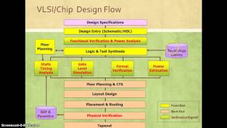
Tape-Out Sign-Off
Interactive Audio Lesson
Listen to a student-teacher conversation explaining the topic in a relatable way.
Introduction to Tape-Out Sign-Off
🔒 Unlock Audio Lesson
Sign up and enroll to listen to this audio lesson

Today, we're going to discuss the Tape-Out Sign-Off. Can anyone tell me what they think Tape-Out means in the context of chip design?

Is it when the design is finalized and ready to be sent for manufacturing?
That's exactly right! Tape-Out refers to the final preparation of a design before it is sent to the foundry. Now, what's the significance of having a sign-off?

I think it ensures that everything is checked and verified before fabrication.
Yes! The sign-off represents a formal approval and aims to catch any last-minute errors.
Verification Processes in Tape-Out Sign-Off
🔒 Unlock Audio Lesson
Sign up and enroll to listen to this audio lesson

In the Tape-Out Sign-Off process, what checks do we typically perform?

DRC, LVS, and ERC checks?
Correct! DRC ensures compliance with design rules, LVS checks the layout versus the schematic, and ERC verifies electrical requirements. Why do you think these checks are essential?

To avoid any potential manufacturing issues that could arise from errors!
Exactly! These verifications help us prevent costly mistakes during fabrication.
Documentation in Tape-Out Sign-Off
🔒 Unlock Audio Lesson
Sign up and enroll to listen to this audio lesson
What kinds of documentation do you think are necessary during the Tape-Out process?
GDSII files and timing reports, perhaps?
Great! The GDSII files contain vital information about the chip's design. Why is it important that these documents are finalized accurately?
If they aren’t accurate, it could lead to fabrication errors!
Exactly! Precise documentation is crucial to ensure that what we designed is what gets fabricated.
Introduction & Overview
Read summaries of the section's main ideas at different levels of detail.
Quick Overview
Standard
The Tape-Out Sign-Off is a critical stage in the VLSI design process, where the design team formally approves the chip design for fabrication. This process involves final checks for compliance with design rules, timing, and power requirements, along with preparing necessary documentation for the foundry.
Detailed
Tape-Out Sign-Off
The Tape-Out Sign-Off is a crucial stage in the physical design verification process, serving as a formal endorsement from the design team that the chip is ready for manufacturing. It necessitates rigorous checks to ensure that the design adheres to all specifications and is feasible for fabrication.
Key Components of Tape-Out Sign-Off:
- DRC, LVS, and ERC Sign-Off: This includes final verification checks that guarantee the design complies with the manufacturing rules and is free of electrical or layout errors, thereby minimizing risks during manufacturing.
- Timing and Power Sign-Off: Ensuring that the design meets specified timing and power requirements across different operating conditions and process corners, vital for chip performance.
- Documentation: This step finalizes all necessary documentation such as GDSII files, timing reports, and power analysis reports to be transmitted to the semiconductor foundry for fabrication.
The significance of this phase lies in its role as a checkpoint, ensuring all verifications are cleared to mitigate the risk of costly errors during the fabrication process.
Youtube Videos


Audio Book
Dive deep into the subject with an immersive audiobook experience.
Definition of Tape-Out Sign-Off
Chapter 1 of 2
🔒 Unlock Audio Chapter
Sign up and enroll to access the full audio experience
Chapter Content
Tape-out sign-off is the formal approval from the design team that the chip design is ready for fabrication. It involves final checks and verifications to ensure the design meets all specifications and that the chip is manufacturable.
Detailed Explanation
Tape-out sign-off is a crucial step in the design process where the design team officially approves the design for manufacturing. Before this sign-off, the design undergoes a series of checks to ensure it aligns with all the necessary specifications. This includes verifying that all the components and connections are correctly placed and functioning as required. Essentially, it confirms that the design is ready to be turned into a physical chip by the semiconductor foundry.
Examples & Analogies
Imagine preparing a recipe before cooking. Before you actually start cooking, you double-check the ingredient list, ensuring that everything is ready and set. Tape-out sign-off functions like that final review—once everything checks out, you’re ready to cook (or in this case, fabricate the chip).
Key Components of Tape-Out Sign-Off
Chapter 2 of 2
🔒 Unlock Audio Chapter
Sign up and enroll to access the full audio experience
Chapter Content
The tape-out sign-off typically includes:
- DRC, LVS, and ERC Sign-Off: Final verification checks to ensure that the design adheres to manufacturing rules and is free of electrical or layout errors.
- Timing and Power Sign-Off: Ensuring that the design meets all timing and power requirements across all process corners and operating conditions.
- Documentation: Finalizing all documentation, including GDSII files, timing reports, and power analysis reports, to be sent to the foundry.
Detailed Explanation
The tape-out sign-off consists of several important checks and documentation processes:
1. DRC, LVS, and ERC Sign-Off: This step ensures that the design follows all necessary manufacturing rules (DRC), matches the intended circuit design (LVS), and meets electrical standards (ERC).
2. Timing and Power Sign-Off: This verification confirms that the circuit operates correctly under various conditions, ensuring it meets all timing and power specifications. This is important since a chip may face different operational conditions after it is built.
3. Documentation: This includes preparing the necessary files and reports that will be sent to the foundry for fabrication. These documents outline all specifications of the design in detail, ensuring that the fabrication process can proceed smoothly without issues.
Examples & Analogies
Consider launching a product in a store. Before it goes on the shelves, you need to make sure it’s safe (like DRC), looks like the design (similar to LVS), and functions as promised without failing (related to ERC). You also need to prepare an instruction manual (documentation) to help consumers understand the product. This thorough preparation ensures that when the product hits the market, everything is in order.
Key Concepts
-
Tape-Out Sign-Off: The formal approval that confirms a chip design is ready for manufacturing.
-
DRC: Ensures design compliance with manufacturing rules.
-
LVS: Verifies that the physical layout matches the design schematic.
-
ERC: Checks for electrical compliance and performance.
Examples & Applications
Example of a DRC violation could be two metal traces that are too close together, potentially causing a short circuit during fabrication.
A case of LVS violation can occur when a transistor in the layout is missing or incorrectly connected compared to the schematic.
Memory Aids
Interactive tools to help you remember key concepts
Rhymes
Before we tape it out, let's check and scout, for any errors that may cause a pout.
Stories
Once upon a time in a design team, they taped out a chip but missed a seam; manufacturing gave an awful scream because errors caused the whole dream to gleam.
Memory Tools
Remember 'D-L-E' for DRC, LVS, and ERC—essential checks before we say, 'Tape-Out is set for the day!'
Acronyms
Use 'SLAP' to remember
Sign-Off
Layout checks
Approval
and Preparations.
Flash Cards
Glossary
- TapeOut
The process of preparing the final design files to be sent to a semiconductor foundry for chip fabrication.
- DRC
Design Rule Checking; a verification method to ensure layouts comply with manufacturing design rules.
- LVS
Layout Versus Schematic; a verification process ensuring that the physical layout matches the schematic design.
- ERC
Electrical Rule Checking; a process that checks electrical behaviors for compliance.
- GDSII
Graphic Data System II; a file format used to represent integrated circuit layouts.
Reference links
Supplementary resources to enhance your learning experience.