
EXERCISES
Enroll to start learning
You’ve not yet enrolled in this course. Please enroll for free to listen to audio lessons, classroom podcasts and take practice test.
Interactive Audio Lesson
Listen to a student-teacher conversation explaining the topic in a relatable way.
Understanding n-Type Semiconductors
🔒 Unlock Audio Lesson
Sign up and enroll to listen to this audio lesson

Today, we'll unpack the characteristics of n-type semiconductors. Can anyone explain what an n-type semiconductor is?

Isn't it a type of semiconductor where electrons are the majority carriers?
Exactly! N-type semiconductors are formed by doping a semiconductor like silicon with pentavalent atoms, such as phosphorus. These atoms provide extra electrons. Can anyone give me an example of a pentavalent dopant?

Phosphorus! It has five valence electrons.
Great job! Remember, n-type means we have negative charges, hence the 'n'. Now, what happens to the number of holes in an n-type semiconductor?

The number of holes is fewer than the number of electrons, right?
Exactly! So we can say that in n-type semiconductors, n is much greater than p. This is critical for understanding conductivity. Can anyone summarize the factors that contribute to n-type conductivity?

The presence of extra electrons from dopants increases conductivity.
Well said! Let's keep this in mind as we discuss p-type semiconductors next.
p-Type Semiconductors Explained
🔒 Unlock Audio Lesson
Sign up and enroll to listen to this audio lesson

Now, who can explain what a p-type semiconductor is?
It’s a type where holes are the majority carriers!
Correct! P-type semiconductors are produced by doping a semiconductor with trivalent atoms, like boron. What is important to note about the charge of these trivalent dopants?
They have one less valence electron than the semiconductor atoms.
Right! This absence of an electron creates a vacancy, or a hole, that can move. Can someone remind us about the relationship between electrons and holes in p-type semiconductors?
In p-type, holes are the majority and electron concentration is much less.
Exactly! So, in terms of symbolism, we write p much greater than n. What is the role of these holes in current conductivity?
They behave like positive charges and can move to conduct current.
Great connection! Remember, combining both n-type and p-type semiconductors forms junctions integral to electronic devices.
Formation and Behavior of p-n Junctions
🔒 Unlock Audio Lesson
Sign up and enroll to listen to this audio lesson
Let’s move on to p-n junctions. Can anyone detail how a p-n junction forms?
It forms when p-type and n-type materials are joined together.
Perfect! During the formation, electrons from the n-side and holes from the p-side recombine in the depletion region. What is created because of this process?
The depletion region, which has no free charge carriers.
Exactly! This creates an electric field. Can anyone tell me what happens when we apply forward bias to a p-n junction?
The barrier decreases, allowing current to flow.
Correct! And conversely, what about reverse bias?
The barrier height increases, restricting current flow.
Excellent discussion! A clear understanding of p-n junction behavior is vital for understanding diodes.
Real-World Applications of Semiconductors
🔒 Unlock Audio Lesson
Sign up and enroll to listen to this audio lesson
Now that we understand semiconductors, can someone explain how they are used in real-world applications?
They’re used in diodes and transistors!
Correct! Diodes allow current to flow only in one direction, critical for rectification. What about transistors?
They can amplify signals and act as switches!
Exactly! Semiconductors form the backbone of modern electronics. What do you think would happen if we couldn’t manipulate these properties?
We wouldn’t have many electronic devices we rely on today.
Right! Your understanding of these concepts is crucial as we move into more complex topics. Great work today!
Introduction & Overview
Read summaries of the section's main ideas at different levels of detail.
Quick Overview
Standard
The exercises cover key concepts of semiconductor physics, including distinctions between n-type and p-type semiconductors, the formation of p-n junctions, and their respective behaviors under different biases. Students will deepen their understanding through practical and theoretical problems.
Detailed
Detailed Summary
This section comprises exercises aimed at consolidating students' knowledge of semiconductor electronics. The exercises are categorized into varying levels of difficulty, ranging from fundamental concepts to advanced applications of p-n junctions and semiconductor properties. The primary focus is on:
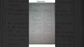
- n-Type and p-Type Semiconductors: Students will explore the differences between these two classifications, learn about their charge carriers, and how doping with trivalent and pentavalent elements influences conductivity.
- p-n Junctions: The formation and significance of p-n junctions in semiconductor devices is addressed, emphasizing how their behavior changes under forward and reverse bias.
- Application of Concepts: Exercises will encourage students to apply theoretical concepts to practical circuits, enhancing their understanding of rectification and current flow in semiconductor devices.
These exercises serve to prepare students for advanced topics in semiconductor technology, ensuring they have a strong grasp of foundational principles.
Youtube Videos


Audio Book
Dive deep into the subject with an immersive audiobook experience.
Exercise 14.1: n-Type Silicon
Chapter 1 of 6
🔒 Unlock Audio Chapter
Sign up and enroll to access the full audio experience
Chapter Content
(a) Electrons are majority carriers and trivalent atoms are the dopants.
(b) Electrons are minority carriers and pentavalent atoms are the dopants.
(c) Holes are minority carriers and pentavalent atoms are the dopants.
(d) Holes are majority carriers and trivalent atoms are the dopants.
Detailed Explanation
In n-type silicon, the majority carriers are electrons, which are present in greater numbers due to the addition of pentavalent dopants (like phosphorus). Electrons are free to move and carry current, while holes (the absence of electrons) are fewer and considered minority carriers. Trivalent atoms do not contribute to the majority charge carriers; they are used in p-type doping.
Examples & Analogies
Think of n-type silicon like a crowded room where people (electrons) are moving freely while a few empty spaces (holes) where someone could stand. The pentavalent atoms act like organizers that bring more people into the room, making the movement of people (current) easier.
Exercise 14.2: p-Type Semiconductors
Chapter 2 of 6
🔒 Unlock Audio Chapter
Sign up and enroll to access the full audio experience
Chapter Content
Which of the statements given in Exercise 14.1 is true for p-type semiconductors?
Detailed Explanation
For p-type semiconductors, holes are the majority carriers, which means they are present in larger numbers due to trivalent doping. The trivalent dopants create holes by not having enough electrons to bond with all neighboring silicon atoms. Electrons become minority carriers in this case.
Examples & Analogies
Imagine a group of friends where most of them (holes) are standing together, while a few are left out (electrons). The trivalent dopants are like extra friends who come without a place in the conversation, creating gaps (holes) where others can fill in.
Exercise 14.3: Energy Band Gaps
Chapter 3 of 6
🔒 Unlock Audio Chapter
Sign up and enroll to access the full audio experience
Chapter Content
Carbon, silicon and germanium have four valence electrons each. These are characterised by valence and conduction bands separated by energy band gaps respectively equal to (E_C), (E_Si) and (E_Ge). Which of the following statements is true?
(a) (E_Si) < (E_Ge) < (E_C)
(b) (E_C) < (E_Ge) > (E_Si)
(c) (E_C) > (E_Si) > (E_Ge)
(d) (E_C) = (E_Si) = (E_Ge)
Detailed Explanation
In semiconductors, different materials have different energy band gaps. Carbon has a larger energy band gap than silicon, which in turn has a larger gap than germanium. This relationship explains their electrical properties and conductivity. The correct statement from the options given is that the energy band gap of silicon is less than that of germanium, and carbon's gap is greater.
Examples & Analogies
Think of each semiconductor as a different bridge. Carbon's bridge is the highest and hardest to cross (high energy gap), silicon's is moderate, and germanium's is the lowest (easiest to cross), which helps to visualize how conduction varies with energy levels.
Exercise 14.4: Unbiased p-n Junction
Chapter 4 of 6
🔒 Unlock Audio Chapter
Sign up and enroll to access the full audio experience
Chapter Content
In an unbiased p-n junction, holes diffuse from the p-region to n-region because (a) free electrons in the n-region attract them. (b) they move across the junction by the potential difference. (c) hole concentration in p-region is more as compared to n-region. (d) All the above.
Detailed Explanation
In a p-n junction, holes naturally diffuse from an area of higher concentration (p-region) to lower concentration (n-region). This movement occurs due to the concentration gradient. While it's true that free electrons attract holes, the primary reason is the concentration gradient difference.
Examples & Analogies
Imagine a crowded elevator (p-region) trying to create space by letting people out into a less crowded hallway (n-region). The natural flow of people reflects the movement of carriers in a semiconductor junction.
Exercise 14.5: Forward Bias in p-n Junction
Chapter 5 of 6
🔒 Unlock Audio Chapter
Sign up and enroll to access the full audio experience
Chapter Content
When a forward bias is applied to a p-n junction, it (a) raises the potential barrier. (b) reduces the majority carrier current to zero. (c) lowers the potential barrier. (d) None of the above.
Detailed Explanation
Applying a forward bias reduces the potential barrier of the p-n junction, allowing more charge carriers to flow through, which results in increased current. This is crucial for semiconductor devices to function, as it facilitates the desired flow of current.
Examples & Analogies
It's like opening a gate that was previously locked (potential barrier) – as soon as you unlock it (apply forward bias), more people (charges) can flow through easily, just like current flowing in a circuit.
Exercise 14.6: Rectification Output Frequency
Chapter 6 of 6
🔒 Unlock Audio Chapter
Sign up and enroll to access the full audio experience
Chapter Content
In half-wave rectification, what is the output frequency if the input frequency is 50 Hz? What is the output frequency of a full-wave rectifier for the same input frequency?
Detailed Explanation
In half-wave rectification, only one half of the AC cycle is used, so the output frequency remains the same as the input frequency, which is 50 Hz. In a full-wave rectifier, both halves of the AC cycle are used, effectively doubling the output frequency to 100 Hz.
Examples & Analogies
Consider pumping water into a tank. Using a half-wave system is like allowing water to flow in only during one direction (like a one-way valve) while a full-wave system manages to pump during both directions, effectively increasing the flow (or output frequency).
Key Concepts
-
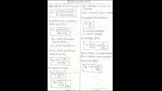
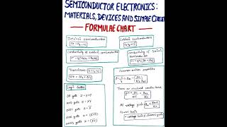
Doping: The process of adding impurities to semiconductors to modify their electrical properties.
-
Charge Carriers: Electrons and holes that carry current in a semiconductor.
-
Depletion Region: The zone around a p-n junction where free charge carriers are absent.
-
Forward Bias: Condition allowing current flow in p-n junction diodes.
-
Reverse Bias: Condition preventing current flow in p-n junction diodes.
Examples & Applications
An example of an n-type semiconductor is silicon doped with phosphorus, providing extra electrons.
An example of a p-type semiconductor is silicon doped with boron, creating holes that can conduct current.
Memory Aids
Interactive tools to help you remember key concepts
Rhymes
N-type for negative charge, electrons in charge—p-type has holes, guiding flows in waves, that’s how it rolls.
Stories
In a quaint village called Silicon, two friends, Nella and Pella, both loved to help their town. Nella brought extra electrons, while Pella made holes that everyone needed to keep the power flowing, making their village shine brightly.
Memory Tools
Remember 'HEN' for n-type: Electrons are the 'H' (Majority), while 'H' stands for holes being minority.
Acronyms
DOP
Doping
Only extra charge carriers
P-type and n-type.
Flash Cards
Glossary
- nType Semiconductor
A semiconductor in which electrons are the majority charge carriers, created by doping with pentavalent elements.
- pType Semiconductor
A semiconductor in which holes are the majority charge carriers, formed by doping with trivalent elements.
- Doping
The intentional introduction of impurities into an intrinsic semiconductor to change its electrical properties.
- Depletion Region
A region at the p-n junction where charge carriers are depleted, resulting in an electric field.
- Forward Bias
A condition in which the p-side of a p-n junction is connected to the positive terminal of a voltage source, allowing current flow.
- Reverse Bias
A condition in which the p-side of a p-n junction is connected to the negative terminal of a voltage source, preventing current flow.
Reference links
Supplementary resources to enhance your learning experience.