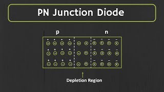
p-n junction diode under reverse bias
Enroll to start learning
You’ve not yet enrolled in this course. Please enroll for free to listen to audio lessons, classroom podcasts and take practice test.
Interactive Audio Lesson
Listen to a student-teacher conversation explaining the topic in a relatable way.
Introduction to Reverse Bias
🔒 Unlock Audio Lesson
Sign up and enroll to listen to this audio lesson

Today, we are going to explore what happens when we apply a reverse bias to a p-n junction diode. Can anyone tell me what reverse bias means?

I think reverse bias means connecting the p-side to a negative voltage and the n-side to a positive one.

Exactly! When we apply reverse bias, we increase the barrier potential across the junction, preventing majority carriers from crossing. What do you think this does to the current?

It probably decreases the current, right?

Yes, it reduces current flow to a negligible amount, primarily allowing only minority carriers to drift across. This leads to a very small current in reverse bias. Can anyone remember what term describes the current that flows in reverse bias?

Is it the reverse saturation current?

Correct! This is very minimal in magnitude. It’s important in preventing damage to the diode. So let’s recap: what influences the behavior of a diode under reverse bias?

The barrier potential and the depletion region width!

Great job, everyone! Remember, understanding reverse bias is critical for circuit applications!
Barrier Potential and Depletion Width
🔒 Unlock Audio Lesson
Sign up and enroll to listen to this audio lesson

Now that we understand reverse bias, let's discuss how it affects the barrier potential and the depletion width. When a reverse bias voltage is applied, what happens to the depletion region?

It widens, right?

Correct! The widening of the depletion region effectively increases the barrier potential, which in turn reduces the current further. Who can explain why current flow is low under reverse bias?

Because the majority carriers are pushed away from the junction!

Exactly, well done! Only minority carriers contribute to current in this scenario. Can anyone give me an example of how understanding reverse bias is useful in electronics?

It helps in designing circuits that can prevent excessive current flow!

Yes, that's a critical application in protecting circuits! Remember, the behavior of a p-n junction under reverse bias is essential in determining how these components function in real-world scenarios.
Reverse Breakdown Voltage
🔒 Unlock Audio Lesson
Sign up and enroll to listen to this audio lesson

Great work so far! Now, let’s discuss breakdown voltage. At what point does reverse bias current sharply increase?

When we reach the breakdown voltage, right?

Correct! When the breakdown voltage is exceeded, the diode can get damaged by excessive current. What measures can we take to prevent this?

We can use current limiting circuits!

Exactly! It’s essential to safely manage current flow. Let’s summarize: how does the reverse bias impact a p-n junction diode in terms of potential and current flow?

Reverse bias increases the potential barrier, widens the depletion region, and allows only a small current until breakdown voltage is reached.

Perfect summary! Well done, everyone. This knowledge is critical for understanding more complex circuits.
Introduction & Overview
Read summaries of the section's main ideas at different levels of detail.
Quick Overview
Standard
When a p-n junction diode is reverse biased, the applied voltage increases the barrier potential, widening the depletion region and minimizing the current flow to that of minority carriers. This behavior is crucial for understanding the diode's functionality in electronic circuits.
Detailed
Overview
The p-n junction diode operates distinctly under reverse bias conditions. When reverse biased, the diode is connected such that the n-side is at a higher potential compared to the p-side, resulting in crucial changes to the diode's behavior.
Key Points
- Barrier Potential: The applied reverse voltage increases the barrier potential, which prevents current from flowing easily across the junction.
- Depletion Region: The widening of the depletion region under reverse bias leads to a further reduction in the flow of charge carriers, specifically blocking majority carriers while allowing only minimal current due to minority carriers.
- Current Flow: The current observed under reverse bias is primarily due to the drift of minority carriers, making it significantly lower than in forward bias conditions.
- Reverse Current Characteristics: The reverse current remains relatively constant until a critical reverse bias voltage, known as breakdown voltage, is reached. Beyond this point, the current can increase dramatically, risking damage to the diode if not controlled.
Significance
Understanding the reverse bias characteristics of p-n junction diodes is essential as it lays the groundwork for their applications in circuits, especially in rectification and protection circuits against overvoltages.
Youtube Videos


Audio Book
Dive deep into the subject with an immersive audiobook experience.
Reverse Bias Configuration
Chapter 1 of 6
🔒 Unlock Audio Chapter
Sign up and enroll to access the full audio experience
Chapter Content
When an external voltage (V) is applied across the diode such that n-side is positive and p-side is negative, it is said to be reverse biased [Fig.14.15(a)].
Detailed Explanation
In a reverse-bias configuration, the diode is connected to a power source in a way that the positive terminal is connected to the n-type side and the negative terminal to the p-type side. This connection prevents current from flowing through the diode under normal circumstances.
Examples & Analogies
Think of a one-way street that only allows cars to go in one direction. In this analogy, applying reverse bias is like putting up a roadblock for cars trying to enter from the wrong direction. The cars (current) can't go through.
Impact of Applied Voltage on Depletion Region
Chapter 2 of 6
🔒 Unlock Audio Chapter
Sign up and enroll to access the full audio experience
Chapter Content
The applied voltage mostly drops across the depletion region. The direction of applied voltage is the same as the direction of barrier potential.
Detailed Explanation
When reverse bias is applied, the majority charge carriers in the diode move away from the junction, widening the depletion region. The depletion region is a zone devoid of free charge carriers, resulting in an increase in the barrier potential, which opposes the flow of current.
Examples & Analogies
Imagine stretching a rubber band. When you pull on it (apply reverse bias), it becomes tighter and stretches further, just like how the depletion region expands when reverse bias is applied.
Effects of Increased Barrier Height
Chapter 3 of 6
🔒 Unlock Audio Chapter
Sign up and enroll to access the full audio experience
Chapter Content
As a result, the barrier height increases and the depletion region widens due to the change in the electric field.
Detailed Explanation
The increase in barrier height makes it more difficult for charge carriers to cross the junction. In this way, electrons from the n-side and holes from the p-side are prevented from recombining, contributing to a significant drop in the diffusion current.
Examples & Analogies
Think of a dam holding back water. The higher the dam (or barrier), the more difficult it is for the water to overflow (or for the current to flow).
Current Behavior under Reverse Bias
Chapter 4 of 6
🔒 Unlock Audio Chapter
Sign up and enroll to access the full audio experience
Chapter Content
The drift current is of the order of a few mA. This is quite low because it is due to the motion of carriers from their minority side to their majority side across the junction.
Detailed Explanation
In reverse bias, although there is some current, it is mainly due to the drift of minority carriers. The current is relatively small and often remains steady regardless of the voltage until it reaches the breakdown voltage.
Examples & Analogies
This is akin to a small trickle of water slowly seeping through a small crack in a dam; it’s not much, but it’s still there until something (breakdown voltage) causes it to burst through.
Breakdown Voltage
Chapter 5 of 6
🔒 Unlock Audio Chapter
Sign up and enroll to access the full audio experience
Chapter Content
The current under reverse bias is essentially voltage independent up to a critical reverse bias voltage, known as breakdown voltage (V_br).
Detailed Explanation
This breakdown voltage is the point where the diode can undergo significant current flow due to a sudden increase in reverse bias, potentially leading to damage. Before this point, the current remains it low levels, independent of further increases in the voltage.
Examples & Analogies
Think of a balloon being inflated; it remains firm until a certain pressure point is reached. Once the pressure exceeds that point, the balloon bursts. Likewise, if the applied reverse voltage exceeds the breakdown voltage, the diode may get destroyed.
Limitations and Considerations
Chapter 6 of 6
🔒 Unlock Audio Chapter
Sign up and enroll to access the full audio experience
Chapter Content
If the reverse current is not limited by an external circuit below the rated value (specified by the manufacturer) the p-n junction will get destroyed.
Detailed Explanation
This emphasizes the need for caution when using diodes under reverse bias. If the reverse current continues to increase past a safe level due to high reverse voltage, it can cause thermal damage and destruction of the diode.
Examples & Analogies
It's like a fuse in a circuit; if too much current flows through it, the fuse can blow to prevent further damage. Similarly, overloading a diode can cause it to fail.
Key Concepts
-
Reverse Bias: This occurs when the p-side of the diode is at a lower potential than the n-side, increasing the depletion region and barrier potential.
-
Depletion Region: An area around the junction where free charge carriers are depleted due to recombination, critical for diode operation.
-
Breakdown Voltage: The reverse voltage at which the diode experiences a sudden increase in current, potentially leading to damage.
Examples & Applications
In a silicon diode, applying a reverse voltage of -5V widens the depletion region significantly, limiting the current to the order of μA, primarily due to minority carriers.
When reverse bias voltage exceeds the breakdown voltage of a diode, it may result in a current that can damage the component if not limited.
Memory Aids
Interactive tools to help you remember key concepts
Rhymes
In reverse the barrier grows, with high potential it shows, but only the weak minority flows!
Stories
Imagine a bustling market (majority carriers) suddenly declaring a stretch where only quiet shoppers (minority carriers) may pass through the gate (depletion region), increasing security (barrier potential).
Memory Tools
D - Depletion region wide, B - Barrier potential high, M - Minimal flow of current.
Acronyms
DRB - Depletion Region Barrier
Represents the impact of reverse bias.
Flash Cards
Glossary
- Reverse Bias
A condition where the p-side of a diode is connected to the negative terminal and the n-side to the positive terminal, increasing the barrier potential.
- Depletion Region
The region around the p-n junction devoid of free charge carriers due to the recombination of electrons and holes, critical in biasing behavior.
- Barrier Potential
The potential difference that opposes the flow of charge carriers, increasing under reverse bias.
- Minority Carrier
Charge carriers (electrons in p-type material and holes in n-type material) present in lower concentration.
- Reverse Saturation Current
The small current that flows across the diode in reverse bias due to minority carriers.
- Breakdown Voltage
The critical reverse voltage at which a diode allows a significant increase in reverse current, potentially leading to damage.
Reference links
Supplementary resources to enhance your learning experience.
