
p-n junction formation
Enroll to start learning
You’ve not yet enrolled in this course. Please enroll for free to listen to audio lessons, classroom podcasts and take practice test.
Interactive Audio Lesson
Listen to a student-teacher conversation explaining the topic in a relatable way.
Concept of p-n Junction
🔒 Unlock Audio Lesson
Sign up and enroll to listen to this audio lesson

Today, we will learn about the formation of a p-n junction. Can anyone tell me what a p-n junction is?

Isn't it where p-type and n-type materials meet?
Exactly! It's formed when a p-type semiconductor, which has more holes, is combined with an n-type semiconductor, which has more electrons. These two types help in controlling electrical currents.

What happens at the junction?
Great question! At the junction, diffusion and drift processes occur, which we will discuss next.
Diffusion in P-N Junction
🔒 Unlock Audio Lesson
Sign up and enroll to listen to this audio lesson

Let’s dive into diffusion. When we have a p-n junction, electrons will start to move from the n-side to the p-side, right?

Yeah, because the electrons want to go where there are fewer of them!
Correct! This movement creates a diffusion current. Now, what do you think happens to the holes in the p-type material during this process?

Holes would move towards the n-region?
Exactly! Holes drift towards areas with fewer holes, and together, these processes create the depletion region.
Drift Current in P-N Junction
🔒 Unlock Audio Lesson
Sign up and enroll to listen to this audio lesson
After diffusion, we have the drift current. Does anyone know what causes this current?
Is it caused by the electric field set up after charge separation?
Correct! The electric field created by the positive space charge on the n-side and negative space charge on the p-side causes the drift of carriers.
So would the drift current oppose the diffusion current?
Yes, very astute! This balancing act continues until the two currents equal each other, establishing equilibrium at the junction.
Equilibrium in a P-N Junction
🔒 Unlock Audio Lesson
Sign up and enroll to listen to this audio lesson
Now that we understand diffusion and drift, let's discuss what happens when they reach equilibrium. Can anyone describe the situation?
The diffusion current equals the drift current, and then there’s no net current, right?
Exactly! This condition leads to the establishment of a potential barrier that prevents further flow of charge carriers.
And why is this potential barrier important?
Great question! The potential barrier is crucial for semiconductor devices, controlling how they conduct electricity in circuits.
Applications of P-N Junctions
🔒 Unlock Audio Lesson
Sign up and enroll to listen to this audio lesson
To wrap up, let's talk about the applications of p-n junctions. Can anyone name a device that uses p-n junctions?
Diodes and transistors!
Correct! P-n junctions are key components in diodes, which allow current to flow in one direction, and transistors, which act as switches and amplifiers in circuits.
So without p-n junctions, modern electronics wouldn't function?
Exactly! They are foundational to the operation of most electronic devices today.
Introduction & Overview
Read summaries of the section's main ideas at different levels of detail.
Quick Overview
Standard
This section explains how a p-n junction is formed by combining p-type and n-type semiconductors, detailing the roles of diffusion and drift currents during the process. It also describes the significance of the depletion region and the electrical characteristics that develop at the junction.
Detailed
Detailed Summary
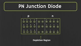
The p-n junction is a fundamental component in semiconductor electronics, formed by joining p-type and n-type semiconductor materials. The process starts with a p-type silicon (Si) wafer, where an appropriate amount of pentavalent impurities is introduced to create an n-type region within it. This creates a metallurgical junction, where two important processes occur: diffusion and drift.
In diffusion, electrons migrate from the n-type region (where they are in higher concentration) to the p-type region, while holes move from the p-type region to the n-type region. This movement of charge carriers establishes a diffusion current across the junction. Meanwhile, as electrons leave the n-region, they generate a positive charge (due to ionized donor atoms), and as holes move from the p-side, they create a negative charge (from ionized acceptors). Together, these reactions lead to the formation of a depletion region, devoid of free charge carriers, characterized by immobile ion cores.
As the depletion region expands, an electric field is established, which causes a drift current opposite to the diffusion current. This process continues until the drift current is equal to the diffusion current, indicating the formation of an equilibrium state in the junction with no net current flow. The p-n junction is essential for the operation of devices such as diodes and transistors, as the potential barrier established across the junction controls the current flow based on external voltage application.
Youtube Videos


Audio Book
Dive deep into the subject with an immersive audiobook experience.
Formation of P-N Junction
Chapter 1 of 4
🔒 Unlock Audio Chapter
Sign up and enroll to access the full audio experience
Chapter Content
Consider a thin p-type silicon (p-Si) semiconductor wafer. By adding precisely a small quantity of pentavalent impurity, part of the p-Si wafer can be converted into n-Si. There are several processes by which a semiconductor can be formed. The wafer now contains p-region and n-region and a metallurgical junction between p- and n- region.
Detailed Explanation
A p-n junction is formed by taking a p-type silicon wafer and introducing a small amount of pentavalent impurity (e.g. phosphorus) to create an n-type region. The p-type region has an abundance of holes (positive charge carriers), while the n-type region has a high concentration of electrons (negative charge carriers). This creates two distinct areas on the wafer, crucial for the formation of the junction where these two types meet.
Examples & Analogies
Think of the p-n junction like a sandwich where the p-type is the lettuce and the n-type is the tomato. Adding the tomato (n-type) to the lettuce (p-type) creates a unique combination that has distinct properties, much like how the junction will behave differently than either region alone.
Diffusion and Drift
Chapter 2 of 4
🔒 Unlock Audio Chapter
Sign up and enroll to access the full audio experience
Chapter Content
Two important processes occur during the formation of a p-n junction: diffusion and drift. We know that in an n-type semiconductor, the concentration of electrons (number of electrons per unit volume) is more compared to the concentration of holes. Similarly, in a p-type semiconductor, the concentration of holes is more than the concentration of electrons. During the formation of p-n junction, and due to the concentration gradient across p- and n- sides, holes diffuse from p-side to n-side (p → n) and electrons diffuse from n-side to p-side (n → p). This motion of charge carriers gives rise to diffusion current across the junction.
Detailed Explanation
As the p-n junction is formed, two processes occur simultaneously: diffusion and drift. In diffusion, holes from the p-region move towards the n-region because there are more holes in the p-region due to its composition, leading to a flow of charge carriers. Similarly, electrons from the n-region will move towards the p-region. This results in a diffusion current, as charge carriers are trying to balance the concentration differences between both sides.
Examples & Analogies
Imagine a crowded room (p-type) where some people (holes) are trying to exit to a less crowded area (n-type), while at the same time, people from the less crowded area (electrons) are trying to enter the crowded room. The mixing of these two groups creates movement across the junction, symbolizing how current flows through the p-n junction.
Formation of Depletion Region
Chapter 3 of 4
🔒 Unlock Audio Chapter
Sign up and enroll to access the full audio experience
Chapter Content
When an electron diffuses from n fi p, it leaves behind an ionised donor on n-side. This ionised donor (positive charge) is immobile as it is bonded to the surrounding atoms. As the electrons continue to diffuse from n fi p, a layer of positive charge (or positive space-charge region) on n-side of the junction is developed. Similarly, when a hole diffuses from p fi n due to the concentration gradient, it leaves behind an ionised acceptor (negative charge) which is immobile. As the holes continue to diffuse, a layer of negative charge (or negative space-charge region) on the p-side of the junction is developed.
Detailed Explanation
As electrons and holes move across the junction, they leave behind positively charged donors (from the n-side) and negatively charged acceptors (from the p-side). This results in a region devoid of mobile charge carriers, called the depletion region. The immobile charges create an electric field that opposes further movement of charge carriers, shaping the behavior of the junction.
Examples & Analogies
Think of a volleyball game where players leave the court. As players exit (electrons and holes), they leave empty spaces (depletion region) on their team. Those empty spaces create an area where no new players can easily come in without permission, similar to how the electric field prevents further charge carrier movement in a p-n junction.
Equilibrium State
Chapter 4 of 4
🔒 Unlock Audio Chapter
Sign up and enroll to access the full audio experience
Chapter Content
This space-charge region on either side of the junction together is known as depletion region as the electrons and holes taking part in the initial movement across the junction depleted the region of its free charges. The thickness of the depletion region is of the order of one-tenth of a micrometre. Due to the positive space-charge region on n-side of the junction and negative space charge region on p-side of the junction, an electric field directed from positive charge towards negative charge develops.
Detailed Explanation
The depletion region acts as a barrier. As the junction reaches equilibrium, the diffusion current (caused by concentration differences) ultimately equals the drift current (caused by the electric field). At this point, there is no net current flowing through the junction, despite continued movement of charge carriers.
Examples & Analogies
Consider a busy crosswalk where at first, pedestrians (carriers) move freely from one side to another. However, over time, as the area fills, a police officer creates a barrier. Now, only a certain number can cross at a time (similar to equilibrium), making the pedestrian flow steady and controlled across the junction.
Key Concepts
-
P-N Junction: The interface formed by connecting p-type and n-type semiconductors.
-
Diffusion: The process of charge carriers moving from high concentration to low concentration.
-
Drift: The movement of charge carriers caused by an electric field.
-
Depletion Region: The area around the junction that lacks free charge carriers.
-
Equilibrium: The state where diffusion current equals drift current.
Examples & Applications
A p-n junction is formed when a p-type silicon wafer is doped with a small quantity of pentavalent impurities to create an n-type region.
Diffusion of electrons occurs from n-type to p-type while holes diffuse from p-type to n-type, establishing a depletion region.
Memory Aids
Interactive tools to help you remember key concepts
Rhymes
Diffusion leads to charge release, drift connects them, creating peace.
Stories
Imagine a flowing river where electrons meet holes at the bank, forming a joint, but this area becomes a dry patch, where no fish (carriers) can live - that's the depletion region!
Memory Tools
D for Diffusion, D for Drift, but together they balance – that’s the p-n gift.
Acronyms
P.N.J helps us remember
Potential Barrier
Negative away
Junction action!
Flash Cards
Glossary
- PN Junction
A boundary or interface between p-type and n-type semiconductors.
- Diffusion Current
The current that results from the movement of charge carriers from regions of high concentration to low concentration.
- Drift Current
The current caused by the movement of charge carriers due to an electric field.
- Depletion Region
The region around a p-n junction that is devoid of free charge carriers.
- Potential Barrier
The voltage barrier at a p-n junction that prevents further movement of charge carriers.
Reference links
Supplementary resources to enhance your learning experience.