
EXTRINSIC SEMICONDUCTOR
Enroll to start learning
You’ve not yet enrolled in this course. Please enroll for free to listen to audio lessons, classroom podcasts and take practice test.
Interactive Audio Lesson
Listen to a student-teacher conversation explaining the topic in a relatable way.
Introduction to Extrinsic Semiconductors
🔒 Unlock Audio Lesson
Sign up and enroll to listen to this audio lesson

Today, we are discussing extrinsic semiconductors. Let’s start with an important question: Why do we need to dope semiconductors in the first place?

Is it to improve their conductivity?
Exactly! Intrinsic semiconductors, like pure silicon and germanium, have limited conductivity, especially at room temperature. By adding a small amount of an impurity—an element with different valency—we can create extrinsic semiconductors that have enhanced electrical properties.

What types of impurities are used for doping?
Good question! We typically use pentavalent dopants like phosphorus or arsenic for n-type semiconductors, which donate electrons. Conversely, trivalent dopants like boron or aluminum are used for p-type semiconductors because they create holes by accepting electrons. Remember: 'n for negative, p for positive'—an easy way to link the type of dopant with the majority carrier.

Can you explain how these dopants affect conductivity?
Certainly! In n-type, the extra electron provided by the pentavalent atom makes it easier for current to flow, while in p-type, the absence of an electron creates a hole which also allows charge movement. It’s like having an empty seat in a bus that others can fill more easily!
In summary, extrinsic semiconductors enhance conductivity through doping, which introduces either electrons or holes as majority carriers.
N-type and P-type Semiconductors
🔒 Unlock Audio Lesson
Sign up and enroll to listen to this audio lesson

Now, let’s take a closer look at n-type and p-type semiconductors. Can anyone remind me what makes n-type unique?
It has more electrons than holes, right?
Exactly! The added electrons from the pentavalent dopants are the majority carriers. So in n-type materials, we write n >> n, meaning the number of electrons greatly exceeds the number of holes.
And what about p-type?
In p-type semiconductors, we have the opposite situation. Here, the holes are the majority carriers because trivalent dopants create vacancies where electrons can fit. So we express this as n << n for p-type—indicating that holes greatly outnumber conduction electrons.
Are there any practical examples of where we use n-type and p-type semiconductors?
Absolutely! In transistors and diodes, we often combine n-type and p-type materials to create junctions, which are fundamental in many electronic devices. Before we wrap this up, why do we need to control the concentration of dopants?

To achieve the desired conductivity for specific applications?
Exactly right! By carefully adjusting the amount of dopant, we can fine-tune the electrical properties to fit our needs. Great discussion today!
Mechanisms of Charge Carrier Movement
🔒 Unlock Audio Lesson
Sign up and enroll to listen to this audio lesson
Next, let’s discuss how doping impacts the movement of charge carriers. Does anyone know what happens to conduction when we dope semiconductor materials?
The conductivity increases?
Yes! When we add dopants, we introduce additional charge carriers—making it easier for current to flow through the material. For n-type semiconductors, those charge carriers are electrons, but what can we say about the holes?
They allow for current flow as well, right?
Correct! In p-type semiconductors, holes flow to form current, essentially behaving like mobile positive charges. A useful analogy is to think of electron movement and hole movement as a game where the 'players' have different values or roles based on their environment.
So, how does temperature affect these semiconductors?
Great question! Temperature can influence the intrinsic and extrinsic charge carriers differently. For instance, in intrinsic semiconductors, more temperature means more thermally generated carriers, while in extrinsic ones, increasing temperature may free some bound electrons but primarily affects the intrinsic carrier generation.
To summarize, charge carrier dynamics in doped semiconductors involve the movement of both extra electrons and holes, depending on whether they're n-type or p-type, and temperature fluctuations can further alter these behaviors.
Introduction & Overview
Read summaries of the section's main ideas at different levels of detail.
Quick Overview
Standard
This section discusses how extrinsic semiconductors are created by introducing specific impurities into intrinsic semiconductors, resulting in n-type and p-type semiconductors with enhanced electrical properties. The implications of doping and the mechanisms of charge carrier generation and movement are explored in detail.
Detailed
In this section, we delve into the concept of extrinsic semiconductors, which are derived from intrinsic semiconductors through a process known as doping. Unlike intrinsic semiconductors, which have limited conductivity and are temperature dependent, extrinsic semiconductors possess significantly improved conductivity due to the addition of impurities, or dopants. Doping introduces either pentavalent elements, which create n-type semiconductors with excess electrons, or trivalent elements, which form p-type semiconductors characterized by a predominance of holes. The section explains how the size and properties of dopant atoms influence semiconductor behavior, defines the differences between n-type and p-type materials, and describes the crucial role of charge carriers in determining electrical conductivity. Overall, understanding the principles of extrinsic semiconductors is essential for grasping the operational mechanisms behind most electronic devices.
Youtube Videos


Audio Book
Dive deep into the subject with an immersive audiobook experience.
Introduction to Extrinsic Semiconductors
Chapter 1 of 4
🔒 Unlock Audio Chapter
Sign up and enroll to access the full audio experience
Chapter Content
The conductivity of an intrinsic semiconductor depends on its temperature, but at room temperature its conductivity is very low. As such, no important electronic devices can be developed using these semiconductors. Hence there is a necessity of improving their conductivity. This can be done by making use of impurities.
Detailed Explanation
Intrinsic semiconductors, like pure silicon (Si) or germanium (Ge), have low conductivity, especially at room temperature. To enhance their conductivity and make them suitable for electronic devices, we can add impurities. This process is crucial because it allows us to create materials that can effectively conduct electricity.
Examples & Analogies
Think of intrinsic semiconductors like plain water, which doesn't conduct electricity well. By adding salt (the impurity), the water becomes saline and conducts electricity better. This is similar to how doping enhances the conductivity of semiconductors.
Doping and Dopants
Chapter 2 of 4
🔒 Unlock Audio Chapter
Sign up and enroll to access the full audio experience
Chapter Content
When a small amount, say, a few parts per million (ppm), of a suitable impurity is added to the pure semiconductor, the conductivity of the semiconductor is increased manifold. Such materials are known as extrinsic semiconductors or impurity semiconductors. The deliberate addition of a desirable impurity is called doping and the impurity atoms are called dopants.
Detailed Explanation
Doping is the process of adding a small amount of impurity to a semiconductor to enhance its electrical conductivity. These impurities, known as dopants, can either donate extra electrons or create holes (vacancies where an electron is missing). Depending on the type of dopant, we can create different types of extrinsic semiconductors.
Examples & Analogies
Imagine adding a few drops of food coloring to plain water. The water changes color and can represent an altered state. Similarly, adding impurities to semiconductors changes their electrical properties significantly, allowing them to conduct more electricity.
Types of Dopants: Pentavalent and Trivalent
Chapter 3 of 4
🔒 Unlock Audio Chapter
Sign up and enroll to access the full audio experience
Chapter Content
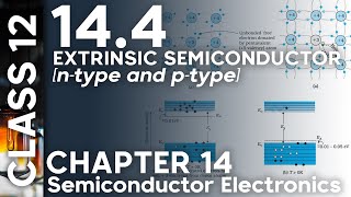
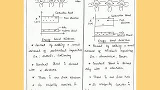
The dopant has to be such that it does not distort the original pure semiconductor lattice. It occupies only a very few of the original semiconductor atom sites in the crystal. A necessary condition to attain this is that the sizes of the dopant and the semiconductor atoms should be nearly the same. There are two types of dopants used in doping the tetravalent Si or Ge: pentavalent (valency 5); like Arsenic (As), Antimony (Sb), Phosphorous (P), etc., and trivalent (valency 3); like Indium (In), Boron (B), Aluminium (Al), etc.
Detailed Explanation
Dopants must closely match the size of the semiconductor atoms to fit into the crystal lattice structure without causing distortion. Pentavalent dopants (which have five valence electrons) contribute additional electrons for conduction, while trivalent dopants (which have three valence electrons) create holes. This difference leads to the formation of n-type and p-type semiconductors, respectively.
Examples & Analogies
Think of a puzzle where the pieces have to fit perfectly together. If you try to force a piece that is too big or too small, it won't fit right. Similarly, dopants must fit well within the semiconductor's structure to effectively change its conductivity.
N-Type and P-Type Semiconductors
Chapter 4 of 4
🔒 Unlock Audio Chapter
Sign up and enroll to access the full audio experience
Chapter Content
Suppose we dope Si or Ge with a pentavalent element. When an atom of +5 valency element occupies the position of an atom in the crystal lattice of Si, four of its electrons bond with the four silicon neighbours while the fifth remains very weakly bound to its parent atom. As a result, the ionisation energy required to set this electron free is very small and even at room temperature it will be free to move in the lattice of the semiconductor. Conversely, a p-type semiconductor is obtained when Si or Ge is doped with a trivalent impurity like Al, B, In, etc.
Detailed Explanation
In n-type semiconductors, the addition of pentavalent dopants results in extra electrons that can move freely, enhancing conductivity. In p-type semiconductors, trivalent dopants create holes by lacking one electron to bond with neighboring silicon atoms. These holes can also conduct electricity, but the nature of conduction is different, focusing on the motion of holes rather than electrons.
Examples & Analogies
Picture a busy road. If more cars (electrons in n-type) enter the road, it becomes more trafficked and conductive. Meanwhile, if there are gaps where cars should be (holes in p-type), those gaps allow movement as others navigate around them. Each type facilitates flow differently but contributes to overall traffic (current).
Key Concepts
-
Doping: The introduction of impurities to enhance conductivity.
-
n-Type Semiconductor: Characterized by extra electrons.
-
p-Type Semiconductor: Characterized by holes created by trivalent impurities.
-
Charge Carriers: Electrons and holes contribute to electrical conduction.
Examples & Applications
When silicon is doped with phosphorus, it becomes an n-type semiconductor due to the excess of free electrons.
When silicon is doped with boron, it becomes a p-type semiconductor, which enhances conductivity through the presence of holes.
Memory Aids
Interactive tools to help you remember key concepts
Rhymes
Doping brings charge to the game, n-types are electrons, p-types have a name!
Stories
Imagine a bus where all the seats are filled with students. Adding more students (dopants) creates more players (electrons or holes) in our semiconductor game, making it easier for them to zip around and share the fun.
Memory Tools
Remember: n = Negative (more electrons) and p = Positive (more holes).
Acronyms
DOP
Doping Of Purity - to remember Dopants for n and p types.
Flash Cards
Glossary
- Extrinsic Semiconductor
A semiconductor whose conductivity is significantly enhanced by the addition of impurities.
- Doping
The process of adding impurities to a semiconductor to change its electrical properties.
- ntype Semiconductor
A type of extrinsic semiconductor that has more electrons than holes, resulting in negative charge carriers.
- ptype Semiconductor
A type of extrinsic semiconductor that has more holes than electrons, resulting in positive charge carriers.
Reference links
Supplementary resources to enhance your learning experience.