
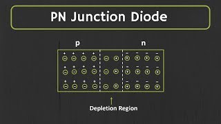
p-n junction diode under forward bias
Enroll to start learning
You’ve not yet enrolled in this course. Please enroll for free to listen to audio lessons, classroom podcasts and take practice test.
Interactive Audio Lesson
Listen to a student-teacher conversation explaining the topic in a relatable way.
Understanding Forward Bias
🔒 Unlock Audio Lesson
Sign up and enroll to listen to this audio lesson

Today, we’re discussing what happens when a p-n junction diode is forward biased. Can anyone explain what we mean by forward bias?

I think it's when the p-side is connected to the positive terminal of the battery and the n-side to the negative terminal?
Exactly! This setup allows current to flow easily through the diode. Remember the acronym FDB? It stands for Forward Bias = Diode conducts current.

So, how does this affect the depletion region?
Great question! The applied voltage reduces the width of the depletion region because it decreases the barrier height that charge carriers must overcome.

So, if I increase the voltage, does the current increase too?
Yes, as you apply a higher voltage, more carriers gain sufficient energy to cross the junction, leading to an increase in current. Remember, this effect is often exponential!
In summary, forward bias decreases the depletion layer and allows carriers to inject across the junction effectively.
Current Flow in Forward Bias
🔒 Unlock Audio Lesson
Sign up and enroll to listen to this audio lesson

Let’s delve deeper into how forward bias affects current flow. What type of current flows when the diode is forward biased?

The majority carrier current, right? Because there are more electrons on the n-side and holes on the p-side.
Not only that! We also have minority carriers contributing to the current. This process is known as minority carrier injection.
Could you explain what that means?
Of course! When voltage is applied, electrons from the n-side move to the p-side where they are in short supply, thus they are 'injected'. Likewise, holes from the p-side move to the n-side.
And this movement creates the total diode forward current, right?
That's correct! Both hole and electron currents combine, giving rise to significant current flow when the diode is forward biased.
To summarize, the forward bias condition allows for substantial minority carrier injection, which leads to a high current.
Barrier Potential and Its Effects
🔒 Unlock Audio Lesson
Sign up and enroll to listen to this audio lesson
Now let’s focus on the relationship between applied voltage and barrier potential. What happens to the barrier potential when we apply forward bias?
The barrier potential decreases, making it easier for charge carriers to cross the junction.
Exactly! To visualize this, think of the barrier as a hill. Applying forward bias flattens the hill, so more carriers can cross easily.
Is there a specific voltage where it starts to allow significant current?
Yes, each diode has a threshold voltage. For example, a silicon diode typically has a threshold voltage around 0.7V. Only beyond this point do we see a rapid increase in current.
Got it! So lower v= lower potential for current.
Exactly! Remember the nickname 'cut-in voltage' for this threshold— it’s the bare minimum required before the diode allows significant current to flow. Let’s recap that the barrier height drops with applied forward bias, leading to increased current and minority carrier movement.
Introduction & Overview
Read summaries of the section's main ideas at different levels of detail.
Quick Overview
Standard
In forward bias, the p-side of a p-n junction diode is connected to the positive terminal of the battery, which decreases the depletion layer width and barrier height, allowing more charge carriers to flow. The relationship between applied voltage and current characteristics are explained, as well as the process of minority carrier injection.
Detailed
When a semiconductor diode is forward biased, the p-side is connected to the positive terminal and the n-side to the negative terminal of the voltage source. This configuration causes the voltage to mostly drop across the depletion region, which has high resistance. Consequently, the depletion region's width decreases, and the effective barrier height is reduced. If the voltage is low, few carriers may cross the junction, leading to a small current; if it is sufficiently high, more carriers can overcome the barrier, increasing current significantly. This behavior demonstrates the diode's rectifying property, allowing current to flow primarily in one direction, a fundamental characteristic that underpins the operation of many electronic devices.
Youtube Videos


Audio Book
Dive deep into the subject with an immersive audiobook experience.
Forward Bias Connection
Chapter 1 of 5
🔒 Unlock Audio Chapter
Sign up and enroll to access the full audio experience
Chapter Content
When an external voltage V is applied across a semiconductor diode such that p-side is connected to the positive terminal of the battery and n-side to the negative terminal, it is said to be forward biased.
Detailed Explanation
In a forward-biased p-n junction diode, the p-side receives a positive charge from the battery while the n-side receives a negative charge. This setup allows charge carriers—holes from the p-side and electrons from the n-side—to move towards the junction.
Examples & Analogies
Think of it like a water pipe in which the p-side is connected to a water source (positive terminal) pushing water (holes) into the pipe, while the n-side (negative terminal) helps remove water (electrons) from the other end.
Effect on Depletion Region
Chapter 2 of 5
🔒 Unlock Audio Chapter
Sign up and enroll to access the full audio experience
Chapter Content
The applied voltage mostly drops across the depletion region and the voltage drop across the p-side and n-side of the junction is negligible. The direction of the applied voltage (V) is opposite to the built-in potential V0.
Detailed Explanation
The forward bias reduces the width of the depletion region—the area around the p-n junction that is devoid of charge carriers. Since the depletion region is where no charges are present and has a high resistance, a smaller region allows for easier flow of current.
Examples & Analogies
Imagine a narrow river that runs through a valley. The application of forward bias is like widening the river, allowing more water to flow freely, thereby significantly increasing the current that can pass through.
Current Flow Under Forward Bias
Chapter 3 of 5
🔒 Unlock Audio Chapter
Sign up and enroll to access the full audio experience
Chapter Content
Due to the applied voltage, electrons from the n-side cross the depletion region and reach the p-side (where they are minority carriers). Similarly, holes from the p-side cross the junction and reach the n-side (where they are minority carriers).
Detailed Explanation
This movement of electrons and holes under forward bias leads to an increase in the overall current flowing through the diode. The process is called minority carrier injection, where carriers inject from one side to the other, increasing the charge carriers in the opposing side.
Examples & Analogies
This is like a crowd at a concert where people (charges) are trying to push through an entrance (junction). If more people enter from the left side (n-side) while others leave from the right (p-side), the overall crowd density increases at the door, symbolizing higher current.
Current Dependency on Voltage
Chapter 4 of 5
🔒 Unlock Audio Chapter
Sign up and enroll to access the full audio experience
Chapter Content
If the applied voltage is small, the barrier potential will be reduced only slightly below the equilibrium value, and only a small number of carriers will possess enough energy to cross the junction. Thus, the current will be small.
Detailed Explanation
At low voltages, only those charge carriers with significant energy can overcome the energy barrier created by the depletion region, resulting in a low current. As the applied forward bias voltage increases, more carriers gain sufficient energy, leading to a significant increase in current flow.
Examples & Analogies
Imagine trying to jump over a small fence (the barrier). If the fence is low (low voltage), only a few can easily get over (small current). But if you increase the pressure (apply more voltage), more people can jump over the fence easily.
Overall Current Description
Chapter 5 of 5
🔒 Unlock Audio Chapter
Sign up and enroll to access the full audio experience
Chapter Content
The total diode forward current is the sum of hole diffusion current and conventional current due to electron diffusion. The magnitude of this current is usually in mA.
Detailed Explanation
The overall current flowing through the diode during forward bias is a combination of two types of movements: one from the holes diffusing into the n-side and the other from electrons moving into the p-side. This results in a current measured in milliamperes (mA), indicating that the diode is effectively conducting.
Examples & Analogies
Think of this current as a busy highway with cars (holes) moving towards a city (p-side) and trucks (electrons) moving towards a rural area (n-side). Both groups contribute to the overall traffic flow, exemplifying how the forward current builds up.
Key Concepts
-
Forward Bias: The condition under which a diode allows significant current to flow.
-
Depletion Region: An area around the pn-junction devoid of charge carriers.
-
Barrier Potential: The voltage needed to overcome the energy field of the depletion region.
Examples & Applications
In a silicon diode, when it is forward biased with a voltage greater than 0.7V, the current increases significantly.
In practical applications, forward biasing is used in circuits to control current flow in one direction.
Memory Aids
Interactive tools to help you remember key concepts
Rhymes
In forward bias, current flows, the junction opens, and energy grows.
Stories
Imagine a toll booth at a one-lane bridge. When fees are paid, the bridge opens; similarly, when a diode is forward biased, it allows 'charge cars' to cross.
Memory Tools
DICE - Depletion Decreases in a Current-Effective forward bias.
Acronyms
BARE - Barrier Abates, Resistance Eases; this will help you remember that barrier potential decreases in forward bias.
Flash Cards
Glossary
- Forward Bias
Condition when the p-side is connected to the positive terminal of a power supply allowing current to flow.
- Barrier Potential
The potential difference across the depletion region that prevents majority carriers from recombining.
- Minority Carrier Injection
The process by which minority carriers are injected into a region with an opposite charge carrier.
- Threshold Voltage (Cutin Voltage)
The minimum voltage that must be applied to the diode before significant current begins to flow.
Reference links
Supplementary resources to enhance your learning experience.