
p-n JUNCTION
Enroll to start learning
You’ve not yet enrolled in this course. Please enroll for free to listen to audio lessons, classroom podcasts and take practice test.
Interactive Audio Lesson
Listen to a student-teacher conversation explaining the topic in a relatable way.
Understanding p-n Junction Formation
🔒 Unlock Audio Lesson
Sign up and enroll to listen to this audio lesson

Today, we’ll explore how a p-n junction is formed. Can someone tell me what happens when p-type and n-type semiconductors are joined?

I think the holes from the p-side and electrons from the n-side will interact.
Exactly! This interaction involves diffusion, where electrons move from n to p and holes move from p to n. Can anyone identify why this movement happens?

It's because of the concentration gradients; there's more of one type of carrier on each side.
Right! This leads to the creation of a depletion region. Remember, we can use the acronym 'D-E-P' to remember: Diffusion, Electric field, and Depletion. What occurs at this depletion region?

There will be an electric field that opposes the movement of charges.
Great observation! The electric field formed counters further diffusion. Let’s summarize: the p-n junction is formed by diffusion, creating a depletion region characterized by an electric field.
Impact of Biasing on p-n Junctions
🔒 Unlock Audio Lesson
Sign up and enroll to listen to this audio lesson

Now, let’s discuss how external voltages impact the p-n junction. What happens when we apply a forward bias?

Connecting the p-side to the positive terminal reduces the barrier potential.
Exactly! This reduction allows current to flow as charge carriers move into the opposite region. Can someone explain what happens under reverse bias?
The depletion region widens, and the barrier increases, which prevents the flow of majority carriers.
Spot on! The drift current of minority carriers still exists, but it’s very small. Let’s remember: ‘F-R-E’ for Forward Reverse Effect! Can someone tell me why we care about reverse bias?
Because it shows how diodes operate as they allow current to flow mostly in one direction.
Exactly! The p-n junction's ability to control current flow between forward and reverse bias is crucial for devices like diodes.
Applications of p-n Junctions
🔒 Unlock Audio Lesson
Sign up and enroll to listen to this audio lesson
Let’s relate our understanding to real-world applications. Who can name a device that uses p-n junctions?
Diodes!
Exactly! Diodes control the direction of current flow. What about transistors—how do they use p-n junctions?
Transistors use both p-n junctions to amplify current!
Well said! They allow small input currents to control larger output currents. Let’s use the memory aid 'T-A-P': Transistor Amplifies Power. Can anyone summarize the applications we've discussed?
p-n junctions are fundamental to diodes and transistors, allowing for precise current control in electronic devices.
Perfect summary! Remember, understanding p-n junctions is key to unlocking the functionality of modern electronics.
Introduction & Overview
Read summaries of the section's main ideas at different levels of detail.
Quick Overview
Standard
This section discusses the formation of a p-n junction through the diffusion and drift of charge carriers between p-type and n-type materials. It covers the behavior of the junction under different external biases, emphasizing its role in semiconductor devices such as diodes and transistors.
Detailed
Detailed Overview of p-n Junctions
The p-n junction serves as the building block for various semiconductor devices, including diodes and transistors. Understanding its formation and behavior under applied voltage is crucial for analyzing semiconductor operations.
Formation of a p-n Junction
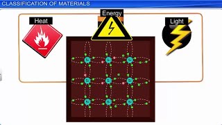
A p-n junction is created when a p-type semiconductor, rich in holes, is joined with an n-type semiconductor, rich in electrons. During the formation process, diffusion occurs due to concentration gradients across the junction. Electrons from the n-side diffuse to the p-side and holes from the p-side diffuse to the n-side, creating a depletion region devoid of free charge carriers. Ionized donor and acceptor atoms remain behind, forming an electric field that counters further diffusion.
Behavior Under Biasing
When an external voltage is applied to the p-n junction, its behavior changes:
- Forward Bias: Connecting the p-side to the positive terminal of the battery reduces the barrier potential, allowing significant current flow as electrons and holes recombine and inject into the opposite regions.
- Reverse Bias: This applies the opposite configuration, widening the depletion region and increasing the barrier potential. The junction allows negligible current flow dominated by minority carriers.
The balance of these currents and electric fields determines the overall functionality of semiconductor devices.
Youtube Videos


Audio Book
Dive deep into the subject with an immersive audiobook experience.
Formation of p-n Junction
Chapter 1 of 4
🔒 Unlock Audio Chapter
Sign up and enroll to access the full audio experience
Chapter Content
A p-n junction is the basic building block of many semiconductor devices like diodes, transistor, etc. A clear understanding of the junction behaviour is important to analyse the working of other semiconductor devices. We will now try to understand how a junction is formed and how the junction behaves under the influence of external applied voltage (also called bias).
Detailed Explanation
The formation of a p-n junction is crucial as it serves as the foundation for many semiconductor devices. A p-n junction is created by joining two regions of semiconductor: one doped with p-type material (which has an excess of holes) and the other with n-type material (which has an excess of electrons). When these two materials are brought together, they form the p-n junction, which allows for the control of electron flow under external voltages.
Examples & Analogies
Think of the p-n junction as a doorway between two rooms. On one side, there's a room full of people ('holes') eager to leave. On the other side, there's a room empty except for a few people ('electrons'). When the doorway is opened (by applying a voltage), people from the crowded room move to the empty room, creating a flow of movement (current).
Diffusion and Drift
Chapter 2 of 4
🔒 Unlock Audio Chapter
Sign up and enroll to access the full audio experience
Chapter Content
Two important processes occur during the formation of a p-n junction: diffusion and drift. We know that in an n-type semiconductor, the concentration of electrons (number of electrons per unit volume) is more compared to the concentration of holes. Similarly, in a p-type semiconductor, the concentration of holes is more than the concentration of electrons. During the formation of p-n junction, and due to the concentration gradient across p-, and n- sides, holes diffuse from p-side to n-side (p ➔ n) and electrons diffuse from n-side to p-side (n ➔ p). This motion of charge carries gives rise to diffusion current across the junction.
Detailed Explanation
Diffusion refers to the movement of charge carriers (electrons and holes) due to concentration differences. In a p-n junction, electrons move from the n-type region (where they are plentiful) to the p-type region (where they are fewer) and holes move in the opposite direction. This is called diffusion current. As the carriers diffuse, they leave behind charged ions in their region, creating a space charge region that leads to an electric field, which in turn causes drift of the carriers back across the junction.
Examples & Analogies
Imagine a crowded festival (the p-type side) where people are rushing to an empty field (the n-type side). As people find their way to the empty field, those already there notice some space opening up and rush back, creating a flow of people in both directions. This push and pull between the crowded area and the empty area represents the diffusion and drift of carriers in the p-n junction.
Equilibrium in p-n Junction
Chapter 3 of 4
🔒 Unlock Audio Chapter
Sign up and enroll to access the full audio experience
Chapter Content
Initially, the diffusion current is large and drift current is small. As the diffusion process continues, the space-charge regions on either side of the junction extend, thus increasing the electric field strength and hence drift current. This process continues until the diffusion current equals the drift current. Thus a p-n junction is formed. In a p-n junction under equilibrium there is no net current.
Detailed Explanation
As diffusion occurs, the charges start building up a space-charge region that creates an electric field. This field opposes further diffusion of carriers. Eventually, the rate at which electrons and holes diffuse across the junction becomes equal to the rate at which they are being pushed back by the electric field, leading to a state of equilibrium where no net current flows.
Examples & Analogies
Think of a race where runners are trying to cross a finish line. Initially, many runners (carriers) rush past the line. However, as runners start getting tired and pulled back by the crowd, the flow slows until the number of runners finishing equals the number being held back. At this point, it’s as if a perfect balance is struck, and no one seems to cross the line.
Barrier Potential
Chapter 4 of 4
🔒 Unlock Audio Chapter
Sign up and enroll to access the full audio experience
Chapter Content
The loss of electrons from the n-region and the gain of electron by the p-region causes a difference of potential across the junction of the two regions. The polarity of this potential is such as to oppose further flow of carriers so that a condition of equilibrium exists.
Detailed Explanation
The presence of the electric field due to the accumulated charges creates a potential barrier that opposes the movement of further carriers across the junction. This potential difference is known as the 'barrier potential' and is crucial for the proper functioning of devices that utilize p-n junctions.
Examples & Analogies
Imagine a water slide that is very steep at the start. Only those people with enough energy can slide down; the rest are stuck at the top because they cannot overcome the initial height (the barrier potential). For electrical current to flow in a p-n junction, the applied voltage must overcome this barrier potential.
Key Concepts
-
p-n Junction: A crucial interface in semiconductor devices formed by combining p-type and n-type materials.
-
Depletion Region: The zone around the junction lacking free carriers, essential for barrier formation.
-
Diffusion and Drift: Key processes that determine charge carrier movement across a junction.
Examples & Applications
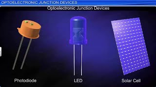
When light is applied to a p-n junction diode, it can generate a current, demonstrating photovoltaic effects.
In transistors, which consist of multiple p-n junctions, small input signals control larger output currents.
Memory Aids
Interactive tools to help you remember key concepts
Rhymes
In a junction where charges play, diffusion and drift show the way, forward bias lets the electrons sway!
Stories
Imagine a town with p and n neighborhoods. They thrive, but when they meet, they create roads (depletion zones) where cars (electrons) travel freely under the right signs (bias).
Memory Tools
D-E-P for the p-n junction: Diffusion leads to an Electric field, creating a Depletion region.
Acronyms
F-R-E stands for Forward Bias Reduces barrier, Reverse Bias Expands it.
Flash Cards
Glossary
- pn Junction
A boundary between p-type and n-type semiconductor materials, critical in semiconductor devices.
- Depletion Region
An area around the p-n junction devoid of free charge carriers, essential for creating a potential barrier.
- Diffusion Current
The current resulting from the movement of charge carriers across the junction due to concentration gradients.
- Drift Current
The current resulting from the movement of charge carriers due to the presence of an electric field.
- Forward Bias
The condition where a positive voltage is applied to the p-side, reducing the junction barrier.
- Reverse Bias
The condition where the p-side is connected to a negative voltage, increasing the junction barrier.
Reference links
Supplementary resources to enhance your learning experience.