
p-type semiconductor
Enroll to start learning
You’ve not yet enrolled in this course. Please enroll for free to listen to audio lessons, classroom podcasts and take practice test.
Interactive Audio Lesson
Listen to a student-teacher conversation explaining the topic in a relatable way.
Introduction to P-type Semiconductors
🔒 Unlock Audio Lesson
Sign up and enroll to listen to this audio lesson

Today, we are going to discuss p-type semiconductors. Does anyone know what it means to be a p-type semiconductor?

Is it related to some type of impurity added to a semiconductor?
Exactly! A p-type semiconductor is created by doping a pure semiconductor, like silicon, with trivalent impurities. Can anyone name a trivalent dopant?

Boron?
Correct! Boron is a common trivalent dopant. What happens at the atomic level when we introduce boron to silicon?

Boron can't form a complete bond because it has one less valence electron.
That's it! This creates holes in the crystal lattice. Remember, a hole acts as a positive charge carrier. We'll use the acronym H for 'Holes = High concentration' to help remember this.

So, holes are the majority carriers in p-type semiconductors?
Yes, that's right! Now, can someone explain why holes are considered effective for conducting electricity?
Because they allow electrons from neighboring atoms to jump to fill the vacancy, creating a flow of positive charges.
Excellent! This process of electron movement makes holes vital for the conduction process in p-type semiconductors.
Charge Carrier Dynamics
🔒 Unlock Audio Lesson
Sign up and enroll to listen to this audio lesson

Now that we understand the basics of p-type semiconductors, let’s discuss the dynamics of charge carriers. Who can tell me about the relationship between the concentration of holes and electrons in a p-type semiconductor?
There are more holes than electrons, right?
That's correct! In fact, we represent this as n >> n, where n stands for holes and n stands for electrons. Why is having a higher number of holes beneficial?
It allows for better control over electrical current flow!
Exactly! In p-type semiconductors, the high concentration of holes makes them efficient for conducting electric currents. This is essential for devices like diodes and transistors.
How does that relate to their use in electronic devices?
Great question! Since holes can facilitate current flow, p-type materials are perfect for applications where we need to control current, such as signal amplification and rectification. So remember, 'P-type = Positive flow!'
Significance of P-type Semiconductors
🔒 Unlock Audio Lesson
Sign up and enroll to listen to this audio lesson
Let’s wrap up our discussion on p-type semiconductors by looking at their significance in today's technology. Can you think of some devices that utilize p-type materials?
Diodes and transistors?
Exactly! P-type semiconductors are essential components in diodes, transistors, and integrated circuits. Why do you think they play such a crucial role?
Because they allow for the control of current flow and signal amplification!
Right you are! The use of p-type materials enables efficient switching and amplification of electrical signals. We can remember this with the phrase 'P-type Power in devices!'
So without p-type, many of our electronics wouldn’t work as well?
Absolutely! The advancements in electronic technology heavily rely on these semiconductors, allowing for smaller and more efficient devices. Keep that in mind as you further explore electronics!
Introduction & Overview
Read summaries of the section's main ideas at different levels of detail.
Quick Overview
Standard
In p-type semiconductors, trivalent atoms such as boron or aluminum are introduced into a tetravalent semiconductor like silicon or germanium, allowing holes to form when a valence electron is absent. This doping process creates a higher concentration of holes than electrons, leading to characteristic electrical properties suitable for various electronic applications.
Detailed
p-type Semiconductor
Introduction to p-type Semiconductors
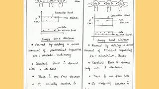
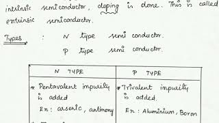
In semiconductor technology, a p-type semiconductor is formed by doping a tetravalent semiconductor, such as silicon (Si) or germanium (Ge), with trivalent impurity atoms. These trivalent elements, such as boron (B), aluminum (Al), or indium (In), have one less valence electron than the semiconductor material. As a result, they create 'holes' where an electron would normally exist.
Formation of Holes
When a trivalent impurity occupies a site in the semiconductor lattice, it can form covalent bonds with three neighboring silicon atoms, but it cannot complete the bond with a fourth silicon atom, leading to an unoccupied bond or a hole. This hole behaves as an effective positive charge carrier and can facilitate the flow of electric current when an electric field is applied.
Charge Carrier Dynamics
In p-type semiconductors, holes are the majority charge carriers, and their concentration is higher than the concentration of electrons (the minority carriers). The relationship can be summarized as:
n >> n (where n represents holes concentration and n represents electron concentration). This means that devices made from p-type semiconductors can control current flow more efficiently due to the abundant availability of holes.
Significance and Applications
P-type semiconductors play an essential role in electronic devices such as diodes, transistors, and integrated circuits. By understanding the properties of p-type materials, engineers can design efficient electronic components that harness the movement of holes for various applications, including signal amplification and rectification.
Youtube Videos


Audio Book
Dive deep into the subject with an immersive audiobook experience.
Introduction to p-type Semiconductors
Chapter 1 of 4
🔒 Unlock Audio Chapter
Sign up and enroll to access the full audio experience
Chapter Content
This is obtained when Si or Ge is doped with a trivalent impurity like Al, B, In, etc. The dopant has one valence electron less than Si or Ge and, therefore, this atom can form covalent bonds with neighbouring three Si atoms but does not have any electron to offer to the fourth Si atom. So the bond between the fourth neighbour and the trivalent atom has a vacancy or hole.
Detailed Explanation
A p-type semiconductor is created by adding a trivalent impurity to silicon (Si) or germanium (Ge). These trivalent atoms have three valence electrons, which means they can form bonds with three surrounding silicon or germanium atoms. However, they leave one bond incomplete since they lack a fourth electron. This results in a ‘hole’, which is essentially a spot in the crystal lattice where an electron is missing. The presence of holes allows for electrical conduction since they can move through the lattice.
Examples & Analogies
Think of a classroom where every student (representing silicon atoms) has a desk. If a new student (the trivalent dopant) joins but doesn’t have a desk for one hand, he can only interact with three students at their desks but leaves one space empty. This empty space is like a hole and can be filled by another student moving over, which helps with the communication flow in the class just like holes assist in current flow.
Conduction Mechanism in p-type Semiconductors
Chapter 2 of 4
🔒 Unlock Audio Chapter
Sign up and enroll to access the full audio experience
Chapter Content
Since the neighbouring Si atom in the lattice wants an electron in place of a hole, an electron in the outer orbit of an atom in the neighbourhood may jump to fill this vacancy, leaving a vacancy or hole at its own site. Thus the hole is available for conduction.
Detailed Explanation
In p-type semiconductors, the holes created due to dopants can move, allowing for electrical conduction. When an electron from an adjacent silicon atom moves to fill the hole, it creates a new hole in its original position. This process of electron movement helps in the conduction of electricity as the holes can effectively move through the semiconductor material. Each hole created is equivalent to a positive charge carrier, meaning that the movement of holes can also be treated as a current.
Examples & Analogies
Imagine a game of musical chairs. Each time a person (electron) moves to fill an empty chair (hole), they create a new empty chair for someone else to fill. Just as participants keep moving to fill chairs, thus maintaining the flow of people, electrons moving to fill holes maintain the flow of electric current in the material.
Majority and Minority Carriers in p-type Semiconductors
Chapter 3 of 4
🔒 Unlock Audio Chapter
Sign up and enroll to access the full audio experience
Chapter Content
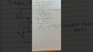
Note that the trivalent foreign atom becomes effectively negatively charged when it shares fourth electron with neighbouring Si atom. Therefore, the dopant atom of p-type material can be treated as core of one negative charge along with its associated hole as shown in p-type material.
Detailed Explanation
In p-type semiconductors, since the trivalent dopants form one hole with neighbouring silicon atoms, they act as 'acceptors'. The trivalent atom effectively takes on a negative charge when it shares its lone electron with silicon. This means that in p-type semiconductors, holes become the majority carriers, which are responsible for carrying positive charge, while the electrons originating from the silicon itself are the minority carriers.
Examples & Analogies
Think of a factory where most employees (holes) are working hard, but there are only a few people (electrons) available to help. The few helpers represent minority carriers, while the majority of the workers (holes) represent the carriers that actually drive productivity in the factory. The work done by the majority is what keeps operations running smoothly.
Charge Carrier Concentration in p-type Semiconductors
Chapter 4 of 4
🔒 Unlock Audio Chapter
Sign up and enroll to access the full audio experience
Chapter Content
Thus, for such a material, the holes are the majority carriers and electrons are minority carriers. Therefore, extrinsic semiconductors doped with trivalent impurity are called p-type semiconductors.
Detailed Explanation
In conclusion, p-type semiconductors are characterized by the presence of holes as the majority carriers resulting from the addition of trivalent impurities. This process leads to a higher concentration of holes compared to electrons, which are termed minority carriers. The ability of p-type semiconductors to conduct electricity primarily through the movement of holes makes them crucial for various applications in electronics.
Examples & Analogies
Consider a busy street where a few bicycles (representing minority carriers) try to navigate through a crowd of pedestrians (representing majority carriers or holes). The street is predominantly filled with the crowd, representing the higher concentration of holes which allow for movement and interactions to occur, illustrating how these charge carriers support conductivity in p-type materials.
Key Concepts
-
P-Type Semiconductors: Created by doping tetravalent semiconductors with trivalent impurities.
-
Holes as Charge Carriers: In p-type semiconductors, holes act as the majority carriers facilitating current flow.
-
Doping Process: The deliberate addition of impurities to modify the electrical properties of semiconductors.
Examples & Applications
Boron is a common trivalent dopant used in silicon to form a p-type semiconductor.
When boron is added to silicon, it creates holes that enable electrical conduction.
Memory Aids
Interactive tools to help you remember key concepts
Rhymes
If you want positive flow, p-type is the way to go!
Stories
In a land of silicon, boron arrived with friends and created holes that allowed electricity to dance and flow freely.
Memory Tools
Remember 'P' for 'positive carriers' to recall what p-type stands for.
Acronyms
Use 'PotoH' to recall that P-type materials promote the movement of Holes.
Flash Cards
Glossary
- ptype semiconductor
A type of semiconductor created by doping a material with trivalent impurities, resulting in a predominance of holes as charge carriers.
- hole
A vacancy in a semiconductor lattice that behaves as a positive charge carrier, formed when an electron is absent.
- doping
The process of adding impurities to a semiconductor to change its electrical properties.
- trivalent impurity
A type of impurity atom with three valence electrons that creates holes in the semiconductor material.
- carrier concentration
The number of charge carriers (holes or electrons) per unit volume in a semiconductor material.
Reference links
Supplementary resources to enhance your learning experience.