
Substrate Preparation
Interactive Audio Lesson
Listen to a student-teacher conversation explaining the topic in a relatable way.
Introduction to Substrate Preparation
🔒 Unlock Audio Lesson
Sign up and enroll to listen to this audio lesson

Today, we’ll be discussing substrate preparation, a critical first step in FinFET fabrication. Can anyone tell me what substrate options we have?

Is it just silicon?
Great question, Student_1! We can use Silicon-on-Insulator, often abbreviated as SOI, or bulk silicon wafers. SOI has advantages due to the insulating layer. Why do you think that’s important?

I think it might help reduce interference from the substrate?
Exactly! That insulating layer minimizes parasitic capacitance, which improves device performance. Let's keep this in mind as we move forward in our studies.
Comparing SOI and Bulk Silicon
🔒 Unlock Audio Lesson
Sign up and enroll to listen to this audio lesson

Now that we know about the substrates, let’s compare SOI and bulk silicon. Student_3, can you mention a benefit of using SOI?

SOI devices have better isolation from parasitic elements.
Correct! And what do you think could be a downside to using SOI?

Maybe it’s more expensive or harder to produce?
That's an excellent point, Student_4. While SOI offers some fantastic benefits, the cost of materials and processes can be higher compared to bulk silicon. Remember this as we proceed with the fabrication techniques in later sessions.
Introduction & Overview
Read summaries of the section's main ideas at different levels of detail.
Quick Overview
Standard
This section outlines substrate preparation as the foundational step in the FinFET fabrication process, highlighting the materials used, specifically Silicon-on-Insulator (SOI) and bulk silicon wafers, and setting the stage for further steps in the FinFET manufacturing process.
Detailed
Substrate Preparation in FinFET Fabrication
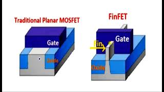
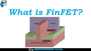
Substrate preparation is the essential first step in the FinFET (Fin Field Effect Transistor) fabrication process. The fabrication begins with selecting the appropriate substrate material, either a Silicon-on-Insulator (SOI) wafer or a bulk silicon wafer.
Using SOI can enhance the electrical properties and performance of the FinFET devices due to the insulating layer that reduces parasitic capacitance, while bulk silicon can be more economical and easier to process at scale. This section emphasizes the importance of this preparatory stage in establishing a stable and reliable base for subsequent processes like fin patterning and etching, gate stack formation, and other essential steps that follow in FinFET device manufacturing.
Youtube Videos

Audio Book
Dive deep into the subject with an immersive audiobook experience.
Starting Materials
Chapter 1 of 2
🔒 Unlock Audio Chapter
Sign up and enroll to access the full audio experience
Chapter Content
Start with a Silicon-on-Insulator (SOI) or bulk silicon wafer.
Detailed Explanation
In the beginning of the FinFET fabrication process, we need to select the right substrate. A Silicon-on-Insulator (SOI) wafer has a layer of silicon on top of an insulating layer, which helps in reducing parasitic capacitance and improving device performance. Alternatively, a bulk silicon wafer can be used, which is simply a solid piece of silicon without the insulating layer. The choice between SOI and bulk silicon can affect how the device performs and its scalability to smaller nodes.
Examples & Analogies
Think of the substrate as the foundation of a building. Just as the type of foundation (concrete slab, pilings, etc.) determines how the structure will stand and respond to forces, the selection of a silicon substrate influences how the FinFET behaves in an electronic circuit.
Importance of Substrate Choice
Chapter 2 of 2
🔒 Unlock Audio Chapter
Sign up and enroll to access the full audio experience
Chapter Content
Choosing the substrate impacts device performance and scaling.
Detailed Explanation
The choice of substrate is crucial for the overall performance of the FinFET. SOI substrates are favored in advanced technology nodes as they help reduce leakage currents and provide better electrostatic control. On the other hand, bulk silicon can be more cost-effective and easier to work with at larger scales, but may lead to higher parasitic effects. As technology nodes shrink, the impact of the substrate on performance becomes more pronounced.
Examples & Analogies
Imagine trying to grow a garden. If you plant your seeds in nutrient-rich soil (equivalent to SOI), they will likely thrive better than if planted in rocky or insufficient soil (similar to bulk silicon), which may lead to stunted growth. The choice of soil affects not only the yield but also the health of the plants.
Key Concepts
-
Substrate Preparation: The foundational step in FinFET fabrication which utilizes SOI or bulk silicon.
-
Silicon-on-Insulator (SOI): A substrate type that provides better electrical properties due to an insulating layer.
-
Bulk Silicon: A more economical substrate option without the benefits of an insulating layer.
Examples & Applications
Using SOI in FinFETs can lead to reduced leakage current due to better isolation.
Bulk silicon wafers are widely used in production due to their cost-effectiveness and ease of handling.
Memory Aids
Interactive tools to help you remember key concepts
Rhymes
SOI is nice, keeps devices precise; bulk silicon costs less, but may cause some stress.
Stories
Imagine a builder choosing between a high-tech insulated foundation and a simple ground slab. The choice affects everything above!
Memory Tools
Remember: 'S' for 'Silicon-on-Insulator' is for 'Superior' performance in FinFETs.
Acronyms
SoB - 'SOI vs Bulk' to remember the two substrate types.
Flash Cards
Glossary
- SilicononInsulator (SOI)
A semiconductor fabrication technique that uses a layered structure of silicon, insulator, and silicon for improved performance.
- Bulk Silicon
A standard silicon wafer without any insulating layer, commonly used in semiconductor manufacturing.
Reference links
Supplementary resources to enhance your learning experience.