
FinFET Device Structure and Operation
Interactive Audio Lesson
Listen to a student-teacher conversation explaining the topic in a relatable way.
Introduction to FinFETs
🔒 Unlock Audio Lesson
Sign up and enroll to listen to this audio lesson

Welcome everyone! Today, we will explore FinFETs, or Fin Field Effect Transistors. These devices are essential for surpassing the limitations of conventional planar MOSFETs, especially as we approach advanced technology nodes. Can anyone share what they know about MOSFETs?

I know that MOSFETs are used in digital switches and circuits, but as we get smaller, they face issues like leakage.
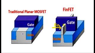
Great point! FinFETs address those issues. They have a 3D structure that helps improve control over the channel. Does anyone know how the structure of a FinFET differs from a planar MOSFET?

I think FinFETs have a vertical channel, while MOSFETs have a flat one?
Exactly! The vertical fin structure allows the gate to control the channel more effectively, reducing leakage. Let's remember this with the acronym '3D': 'D' for 'Dynamic' gate control and 'D' for 'Decreased' leakage.
FinFET Structure Components
🔒 Unlock Audio Lesson
Sign up and enroll to listen to this audio lesson

Now, let's dive deeper into the structure of a FinFET. The main component is the fin itself, which acts as the channel. Can someone describe the functionality of the gate?

The gate surrounds the fin, right? It controls the current flow.
That's correct! The gate's geometry allows for enhanced electrostatic control. Plus, the gate dielectric insulates the gate from the channel. What materials do you think are used for the dielectric?

I believe high-κ materials are commonly used, like Hafnium Dioxide (HfO₂).
Spot on! These materials help in reducing leakage current further. Can anyone recall the purpose of the Shallow Trench Isolation, or STI, in FinFETs?
It's meant to isolate the transistors, right?
Exactly! This prevents electrical interference between devices. You might remember this with 'SI' for 'Separation Isolators'.
Fabrication Process of FinFETs
🔒 Unlock Audio Lesson
Sign up and enroll to listen to this audio lesson
Next, we'll discuss how FinFETs are fabricated. The process is notably more complex than that of planar MOSFETs. Can anyone name the first step in the fabrication of a FinFET?
Does it start with a Silicon wafer?
Correct! We begin with SOI or bulk silicon wafers. From there, what follows?
Then we pattern and etch to create the fin structure!
Exactly! Advanced lithography techniques are employed. The step involves etching to form tall, thin fins, which is crucial for performance. Can anyone explain how we make the gate stack?
We deposit the dielectric material and the metal for the gate, then use conformal deposition to surround the fin?
Spot on! This conformal layer is essential for ensuring uniformity around the fin. Remember our mnemonic 'Gates Always Need Coverage' to stress the importance of gate formation.
Operating Principles
🔒 Unlock Audio Lesson
Sign up and enroll to listen to this audio lesson
Now, let's explore how FinFETs operate. Like MOSFETs, they function in three key regions: cutoff, linear, and saturation. Can anyone explain what happens in the cutoff region?
In the cutoff region, the gate-source voltage is below the threshold voltage, so there's no conduction.
Perfect! In the linear region, what do we observe?
The FinFET behaves like a resistor since the gate voltage is above the threshold.
Exactly! And finally, in saturation, the channel pinches off. Remember, this pinching leads to saturation current. What advantages do you think this provides?
It leads to reduced leakage and improves performance due to better electrostatic control.
Great insights! Keep in mind the phrase 'Saturation Signals Stability', which captures the essence of FinFET performance.
Advantages and Design Considerations
🔒 Unlock Audio Lesson
Sign up and enroll to listen to this audio lesson
To conclude today's discussion, let's talk about the advantages that FinFET technology brings to the table. Who can list some benefits?
Enhanced short-channel control and lower leakage currents!
Exactly! Also, FinFETs support higher drive currents due to their increased effective channel widths. And with technology scaling below 10 nm, they offer significant advantages over planar MOSFETs. What about design considerations?
We need to consider fin count and spacing for effective density.
Correct! More fins increase current, but the density can be affected. Remember the acronym 'FIND' for 'Fin count, Isolation, Number and Density'. So, in summary, FinFETs are crucial for modern electronics due to their enhanced performance and scalability.
Introduction & Overview
Read summaries of the section's main ideas at different levels of detail.
Quick Overview
Standard
FinFETs are advanced transistors designed to overcome the limitations of traditional planar MOSFETs, particularly in deep sub-micron technologies. This section details the structure, fabrication process, and operating principles of FinFETs, showcasing their advantages in terms of performance and leakage reduction.
Detailed
FinFET Device Structure and Operation
FinFETs, or Fin Field Effect Transistors, are an innovative type of 3D transistor that improve upon the limitations of traditional planar MOSFETs in deep sub-micron technology nodes. This section a detailed exploration of FinFETs, including:
1. FinFET Structure
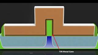
A FinFET incorporates a thin, vertical silicon fin that serves as the channel, surrounded by a gate material on multiple sides. This multi-gate architecture allows for better control over the channel, thus reducing leakage and enhancing device performance. Key components of a FinFET include:
- Fin: The narrow silicon strip forming the channel.
- Gate: Conductive material surrounding the fin.
- Gate Dielectric: An insulating layer, often made of high-κ material, between the gate and fin.
- Source/Drain: Doped regions facilitating current flow on either side of the fin.
- Shallow Trench Isolation (STI): Provides isolation between transistors.
2. Fabrication Process
The fabrication process of a FinFET is more complex compared to standard MOSFETs, involving several steps that leverage advanced lithography and deposition techniques to achieve precise fin geometries:
- Start with a silicon wafer, either SOI or bulk silicon.
- Use lithography to pattern and etch narrow fins.
- Form gate stacks with high-κ dielectrics and metal materials.
- Create spacers and perform source/drain doping.
- Form low-resistance contacts and interconnect metal layers.
3. Key Dimensions
Important dimensions for FinFETs include fin width (W_fin), fin height (H_fin), and gate length (L_g). These dimensions significantly influence the electrostatic control and effective channel width of the FinFETs.
4. Operating Principals
FinFETs operate in three regions: cutoff, linear (Ohmic), and saturation—similar to MOSFETs but with enhanced electrostatic control due to their gate wrapping around the fin, leading to improvements such as reduced leakage currents and better subthreshold swing.
5. Advantages
FinFETs provide significant benefits, including:
- Enhanced short-channel control and reduced DIBL.
- Lower leakage currents due to improved gate control.
- Higher drive currents from larger effective channel widths.
- Scalability for technology nodes of 10nm and below, widely adopted by major foundries.
6. Design Considerations
When designing FinFETs, factors such as fin count, fin pitch, and variability are crucial for device performance and manufacturing efficiency.
Youtube Videos


Audio Book
Dive deep into the subject with an immersive audiobook experience.
Introduction to FinFETs
Chapter 1 of 9
🔒 Unlock Audio Chapter
Sign up and enroll to access the full audio experience
Chapter Content
FinFETs are advanced 3D transistors that address the limitations of traditional planar MOSFETs in deep sub-micron technology nodes.
This chapter explores the detailed structure, fabrication process, and operational principles of FinFETs.
Detailed Explanation
FinFETs, or Fin Field Effect Transistors, represent a significant advancement in transistor technology, designed to overcome the shortcomings associated with traditional planar MOSFETs, particularly as semiconductor technology scales down into smaller nodes (below 10nm). Unlike planar MOSFETs, which have a flat channel, FinFETs feature a three-dimensional structure that allows for better control of the electrical current flow through the device. This chapter will delve into their unique structure, the fabrication steps involved in creating them, and how they operate effectively.
Examples & Analogies
Think of traditional planar MOSFETs as a flat road where cars (electrons) might get stagnant due to traffic (leakage) at certain points; in contrast, FinFETs represent a multi-lane highway, enabling smoother flow and more control of those cars, preventing bottlenecks and improving overall performance.
Structure of FinFETs
Chapter 2 of 9
🔒 Unlock Audio Chapter
Sign up and enroll to access the full audio experience
Chapter Content
A FinFET (Fin Field Effect Transistor) consists of a thin, vertical silicon fin that forms the channel, with the gate wrapping around multiple sides of the fin. This multi-gate geometry enhances control over the channel, reducing leakage and improving performance.
Component Description
- Fin: Narrow strip of silicon forming the channel
- Gate: Conductive material that surrounds the fin on 2 or 3 sides
- Gate Dielectric: Thin insulating layer between gate and fin (often high-κ)
- Source/Drain: Heavily doped regions on either side of the fin
- Shallow Trench Isolation (STI): Used to isolate transistors from each other
Types of FinFETs:
- Double-gate FinFET: Gate on two vertical sides.
- Tri-gate FinFET: Gate wraps around three sides (top + sides).
- Multi-fin FinFET: Multiple fins connected in parallel for increased current handling.
Detailed Explanation
The core structure of a FinFET comprises a vertical silicon fin that acts as the channel where current flows. This fin is uniquely surrounded by gates on multiple sides rather than just one, which allows for enhanced electrostatic control over the channel. The main components include:
- Fin: The narrow strip that creates the channel, crucial for defining the device's electrical properties.
- Gate: A conductive material that wraps around 2 or 3 sides of the fin, improving control and performance.
- Gate Dielectric: A thin insulating layer that separates the gate from the fin, typically made from materials with high dielectric constants (high-κ) for better performance.
- Source/Drain: Heavily doped areas at the ends of the fin that inject and collect charge carriers.
- STI: This is used for isolating different transistors in order to prevent interference between them.
The types of FinFETs vary in terms of their gate structure, with double-gate and tri-gate configurations providing different levels of control and performance, while multi-fin configurations allow for higher current handling.
Examples & Analogies
Imagine a water channel that transports water (electrons) from one place to another. A traditional channel would have walls on only one side (like a standard MOSFET), while a FinFET channel has walls on three sides ensuring better management of the water flow and preventing spills (leakage). The different configurations of gates (double-gate and tri-gate) can be likened to having different styles of channels that optimize how efficiently we can control the flow of water.
FinFET Fabrication Process
Chapter 3 of 9
🔒 Unlock Audio Chapter
Sign up and enroll to access the full audio experience
Chapter Content
- Substrate Preparation
- Start with a Silicon-on-Insulator (SOI) or bulk silicon wafer.
- Fin Patterning and Etching
- Use advanced lithography (EUV/DUV) to define narrow fin structures.
- Etch silicon to form tall, thin fins.
- Gate Stack Formation
- Deposit high-κ dielectric (e.g., HfO₂) and metal gate material.
- Gate wraps around the fin using conformal deposition.
- Spacer Formation and Source/Drain Implantation
- Add spacers beside the gate.
- Dope source and drain regions heavily for conductivity.
- Silicidation and Contacts
- Form low-resistance contacts using metal silicide.
- Interconnects
- Create metal layers for wiring using damascene or dual-damascene processes.
Advanced nodes may use self-aligned patterning, gate-last processing, or EUV lithography to improve accuracy and reduce variation.
Detailed Explanation
The FinFET fabrication process is a multi-step procedure involving:
- Substrate Preparation: Starting with a Silicon-on-Insulator wafer or a bulk silicon wafer is critical as it provides a suitable base for the subsequent steps.
- Fin Patterning and Etching: Advanced lithography techniques are employed to create precise patterns on the wafer surface, after which etching is used to carve out the tall, thin fins necessary for the FinFET design.
- Gate Stack Formation: This step involves layering a high-κ dielectric material and metallic material to form the gate, which must conform to the shape of the fin to ensure effective operation.
- Spacer Formation and Source/Drain Implantation: Spacers are introduced next to the gate, followed by doping the source and drain regions to enhance conductivity.
- Silicidation and Contacts: Creating low-resistance contacts is essential for efficient electrical connection.
- Interconnects: Finally, metal layers are added to establish connections between different FinFETs using techniques like damascene or dual-damascene processing. Advanced lithography techniques are also employed at smaller nodes to minimize variations in the fin dimensions and improve the precision of the overall fabrication process.
Examples & Analogies
Manufacturing FinFET devices is somewhat akin to constructing a small city. You need to prepare the land (substrate), create detailed building plans (fin patterning and etching), and then carefully construct each building (gate formation) ensuring they have necessary connections for utilities (contacts). Just like in urban planning where spaces need to be effectively utilized and organized, FinFET fabrication requires precise dimensions and spacing to ensure optimal performance.
Key Dimensions in FinFETs
Chapter 4 of 9
🔒 Unlock Audio Chapter
Sign up and enroll to access the full audio experience
Chapter Content
| Parameter | Symbol | Description |
|---|---|---|
| Fin Width | Wfin | Determines electrostatic control; thinner = better |
| Fin Height | Hfin | Increases effective channel width (W_eff) |
| Gate Length | Lg | Critical for short-channel control |
| Effective Channel Width | Weff=2×Hfin+Wfin | For a single-fin tri-gate |
Detailed Explanation
The dimensions of a FinFET play a crucial role in determining its performance:
- Fin Width (Wfin): The width of the fin is vital for electrostatic control. Thinner fins provide better control of the channel, leading to improved performance.
- Fin Height (Hfin): The height of the fin contributes to the effective channel width, meaning taller fins can enhance current carrying capability.
- Gate Length (Lg): This parameter is critical for controlling short-channel effects, allowing the device to function correctly at smaller sizes.
- Effective Channel Width (Weff): This is calculated based on the fin height and width, contributing to how well the FinFET can manage current flow.
Examples & Analogies
Consider the dimensions of an elevator shaft in a skyscraper. A wider elevator might carry more people, while a taller shaft allows for quicker movement between floors. Similarly, in FinFETs, a thinner and taller fin effectively allows for better control and higher performance in carrying 'electrons' (the current in this case), much like how a well-designed elevator system enhances operational efficiency.
Operating Principle of FinFETs
Chapter 5 of 9
🔒 Unlock Audio Chapter
Sign up and enroll to access the full audio experience
Chapter Content
Similar to MOSFETs, FinFETs operate in three regions:
- Cutoff: VGS < VTH; no conduction.
- Linear (Ohmic): VGS > VTH, VDS small; behaves like a resistor.
- Saturation (Active): VDS > VGS − VTH; channel pinches off, current saturates.
- Gate voltage (V_GS) controls the depletion/inversion in the fin.
- Because the gate wraps around the fin, electrostatic control is stronger, leading to reduced leakage and better subthreshold swing.
Detailed Explanation
FinFETs function similarly to other types of field-effect transistors but with improved operational characteristics. They have three primary regions of operation:
1. Cutoff: When the gate-to-source voltage (VGS) is less than the threshold voltage (VTH), the FinFET does not conduct, essentially acting as an 'off' switch.
2. Linear (Ohmic): In this region, when VGS is above VTH, and the drain-to-source voltage (VDS) is small, the FinFET behaves like a resistor, allowing current to flow linearly proportional to the voltage applied.
3. Saturation (Active): When VDS exceeds VGS minus VTH, the channel 'pinches off,' causing the current to stabilize and saturate at a constant value.
The surrounding gate structure in FinFETs enhances electrostatic control over the channel, resulting in less leakage current and a better ability to switch on and off efficiently.
Examples & Analogies
Think of a water faucet as FinFET operation. In the Cutoff region, the faucet is completely turned off, preventing any water from flowing. When partially opened (Linear region), water flows steadily like a trickle, and once fully opened (Saturation), the water flow stabilizes at a certain maximum rate even if you turn the faucet knob further. The ability of the faucet to control water flow in these stages mirrors how a FinFET controls the flow of electric current based on the gate voltage.
Advantages of FinFET Operation
Chapter 6 of 9
🔒 Unlock Audio Chapter
Sign up and enroll to access the full audio experience
Chapter Content
✅ Enhanced Short-Channel Control
- Reduced DIBL (Drain-Induced Barrier Lowering)
- Improved subthreshold slope
✅ Lower Leakage Current
- Better gate control → less off-state leakage
✅ Higher Drive Current
- Taller fins provide larger effective channel width
✅ Scalable for 10 nm and beyond
- Used in all major foundries: Intel, TSMC, Samsung
Detailed Explanation
FinFETs possess several key advantages over traditional planar MOSFETs, including:
- Enhanced Short-Channel Control: They experience reduced DIBL, which helps in maintaining transistor performance as size shrinks, resulting in improved subthreshold slopes.
- Lower Leakage Current: The multi-gate structure provides better control over the channel, significantly reducing unwanted current flow when the device is off, thereby minimizing leakage.
- Higher Drive Current: Because of their taller fins, FinFETs offer increased effective channel width, allowing them to carry more current when turned on, which is critical for higher performance applications.
- Scalability: FinFETs are designed for modern fabrication techniques and are suitable for nodes as small as 10 nm, making them the technology of choice for major manufacturers like Intel, TSMC, and Samsung.
Examples & Analogies
Consider FinFET technology like a smart irrigation system for a large farm. It helps ensure that each plant receives the right amount of water (current). Just like how this system minimizes water waste and ensures efficiency, FinFETs improve electrical efficiency, boost performance, and reduce undesirable effects in modern electronics.
FinFET vs MOSFET Operation
Chapter 7 of 9
🔒 Unlock Audio Chapter
Sign up and enroll to access the full audio experience
Chapter Content
| Feature | Planar MOSFET | FinFET |
|---|---|---|
| Channel Geometry | Flat | Vertical fin |
| Gate Control | Single side | Three sides |
| SCE Tolerance | Poor | Excellent |
| I_on/I_off Ratio | Moderate | High |
| Subthreshold Swing | >70 mV/dec | <70 mV/dec |
| Scalability | Limited | Excellent |
Detailed Explanation
When comparing FinFETs and traditional MOSFETs, several features highlight the advantages of FinFET technology:
- Channel Geometry: Unlike the flat channel of a MOSFET, FinFETs employ a vertical fin, which allows for better electrostatic control.
- Gate Control: MOSFETs control the channel from a single side, whereas FinFETs can control it from three sides, enhancing performance.
- Short-Channel Effects (SCE) Tolerance: FinFETs demonstrate excellent tolerance against short-channel effects, which often degrade performance in smaller devices.
- ON/OFF Current Ratio: FinFETs achieve a higher I_on/I_off ratio, making them more efficient in the off-state.
- Subthreshold Swing: With a steeper slope (less than 70 mV/decade), FinFETs show improved performance when transitioning between on and off states.
- Scalability: FinFETs can be scaled down to smaller dimensions more effectively than planar MOSFETs, making them ideal for advanced technologies.
Examples & Analogies
If we think of FinFETs and MOSFETs in terms of vehicle design, a traditional MOSFET would be like a regular sedan, which might struggle with tight turns (short-channel effects). In contrast, a FinFET resembles a modern sports car, expertly designed for efficiency, control, and speed, ensuring superior maneuverability and performance in challenging conditions.
Design Considerations in FinFETs
Chapter 8 of 9
🔒 Unlock Audio Chapter
Sign up and enroll to access the full audio experience
Chapter Content
● Fin Count: More fins increase current but require more area.
● Fin Pitch: Minimum spacing between fins; affects density.
● Quantized Width: Width is discrete based on number of fins.
● Variability: Control of fin dimensions is critical for device matching.
Detailed Explanation
When designing FinFETs, several important factors must be considered:
- Fin Count: Increasing the number of fins improves current capacity but also takes up more area on the chip.
- Fin Pitch: This refers to the spacing between individual fins; having too little space can lead to issues with performance and density of the chips.
- Quantized Width: The width of the fins is not continuous but rather defined by the number of fins used; this can affect how well multiple fins work together.
- Variability: Precise control over fin dimensions is essential to ensure consistent performance across the chip, as mismatched sizes can lead to variability in how the devices function.
Examples & Analogies
Imagine building a multi-lane road system where each lane represents a fin. The number of lanes (fin count) can increase traffic flow, but it also takes up more space (area). If lanes are too close together (fin pitch), they risk accidents (performance issues). The width of each lane (quantized width) determines how many cars can move at once, with a constant careful planning necessary to ensure they all operate efficiently (variability).
Summary of Key Concepts
Chapter 9 of 9
🔒 Unlock Audio Chapter
Sign up and enroll to access the full audio experience
Chapter Content
● FinFETs use a 3D fin-shaped channel and multi-gate control to enhance performance and reduce leakage.
● Fabrication is more complex than planar MOSFETs but enables advanced scaling.
● FinFET operation is similar to MOSFETs but benefits from better electrostatics and drive strength.
● These devices are the standard in 7nm, 5nm, and 3nm CMOS nodes.
Detailed Explanation
In summary, key takeaways regarding FinFET technology include:
- FinFETs incorporate a novel 3D channel and multi-gate control, allowing for superior performance compared to traditional transistors relevant in smaller nodes.
- The fabrication process is intricate compared to planar MOSFETs, reflecting the advanced technologies required for smaller process nodes.
- Their operation shares similarities with traditional MOSFETs but benefits significantly from enhanced electrostatic control which leads to improved performance metrics.
- FinFETs have become the standard for modern semiconductor manufacturing processes, especially in 7nm, 5nm, and 3nm technologies.
Examples & Analogies
Consider FinFETs as the next generation of both smartphones and their underlying technology. Just as modern smartphones boast enhanced features, higher performance, and larger capacities than older models through innovative designs and builds, FinFETs have revolutionized semiconductor technologies to meet the growing demands for efficiency and performance in today's tech landscape.
Key Concepts
-
FinFET Structure: Utilizes a vertical silicon fin that allows better electrostatic control over the channel.
-
Fabrication Process: Involves steps like substrate preparation, fin etching, gate stack formation, and more.
-
Operating Principles: FinFETs operate in cutoff, linear, and saturation regions, similar to MOSFETs.
-
Advantages: FinFETs offer enhanced performance, lower leakage, and are scalable for advanced technology nodes.
Examples & Applications
Example of enhanced performance in FinFETs compared to traditional MOSFETs: A FinFET can operate efficiently at smaller dimensions with fewer instances of leakage current.
Case study on FinFET applications in modern processors, which utilize these transistors to achieve higher speeds and lower power consumption.
Memory Aids
Interactive tools to help you remember key concepts
Rhymes
Fin and gate, together they mate, controlling flow, keeping it straight.
Stories
Once in a silicon castle stood a tall fin surrounded by a protective gate. This castle could control the flow of currents, ensuring stability and efficiency, ruling the realm of transistors.
Memory Tools
Remember 'Gates Are Always Effective' for the key roles of gate structures in transistor performance.
Acronyms
Use 'FIND' to remember
Fin count
Isolation
Number
and Density in FinFET design.
Flash Cards
Glossary
- FinFET
A type of 3D transistor that uses a vertical fin as the channel, improving electrostatic control and reducing leakage.
- Gate
The conductive material surrounding the fin in a FinFET that controls current flow.
- Gate Dielectric
Insulating layer between the fin and gate, often made of high-κ materials.
- Shallow Trench Isolation (STI)
Method for isolating transistors from one another in a semiconductor device.
- Subthreshold Slope
A measure of how effectively a transistor can switch off; a lower value indicates better performance.
- DrainInduced Barrier Lowering (DIBL)
A phenomenon affecting short-channel transistors leading to reduced control over the channel.
Reference links
Supplementary resources to enhance your learning experience.