
Introduction
Interactive Audio Lesson
Listen to a student-teacher conversation explaining the topic in a relatable way.
Introduction to FinFETs
🔒 Unlock Audio Lesson
Sign up and enroll to listen to this audio lesson

Today, we’re discussing FinFETs, the next evolution of transistors. Who can tell me what makes FinFETs different from traditional planar MOSFETs?

I think they have a 3D structure instead of being flat.
Exactly! This 3D structure allows for better control over the channel, which is crucial in smaller technology nodes. Who can share why better control is important?

It helps reduce leakage current and improve performance, right?
Precisely! Remember the acronym LEAP for Leakage, Enhanced performance, and Advance scalability. Let’s delve deeper into why FinFETs are significant in advanced technology nodes.
Advantages of FinFETs
🔒 Unlock Audio Lesson
Sign up and enroll to listen to this audio lesson

What advantages do you think FinFETs provide compared to traditional MOSFETs?

They have better short-channel control!
Correct! Enhanced control leads to reduced Drain-Induced Barrier Lowering, also known as DIBL. Can anyone explain what DIBL means?

It's when the drain voltage affects the threshold voltage, which can lead to unwanted conduction.
Well put! This reduction is critical for maintaining efficiency in smaller nodes. Let’s summarize: FinFETs have lower leakage, higher drive current, and are scalable for advanced nodes. The acronym FRESH can help you remember these benefits.
Future of FinFETs
🔒 Unlock Audio Lesson
Sign up and enroll to listen to this audio lesson
As we wrap up, why do you think FinFETs are essential for the future of semiconductor technology?
Because they’re being used in all major foundries, especially at 7nm and below.
Exactly! This capability allows for design innovation at the nanoscale. If you had to choose one key takeaway about FinFETs, what would it be?
They allow us to use more powerful chips in smaller devices!
Great summary! Remember that FinFET technology is essential for pushing the limits of performance in modern electronics.
Introduction & Overview
Read summaries of the section's main ideas at different levels of detail.
Quick Overview
Standard
This section introduces FinFETs, describing their role as 3D transistors designed to enhance performance and minimize leakage in deep sub-micron technology. The following chapters detail their structure, fabrication processes, and operational principles.
Detailed
Detailed Summary of Section 5.1: Introduction
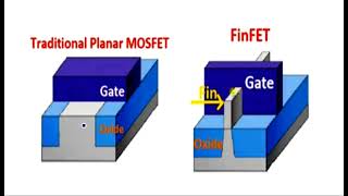
FinFETs, or Fin Field Effect Transistors, are a cutting-edge solution that addresses significant limitations faced by traditional planar MOSFETs, particularly as technology nodes scale down below 10nm. This section sets the groundwork for understanding FinFETs, offering a preview of the subsequent discussions around their intricate structure, fabrication process, and operational principles. In essence, FinFETs incorporate a three-dimensional design that allows for enhanced electrical control, resulting in better performance metrics, reduced leakage currents, and overall improved device scaling capabilities. This chapter aims to provide comprehensive insights into how these advanced devices transform semiconductor technology.
Youtube Videos

Audio Book
Dive deep into the subject with an immersive audiobook experience.
Overview of FinFETs
Chapter 1 of 2
🔒 Unlock Audio Chapter
Sign up and enroll to access the full audio experience
Chapter Content
FinFETs are advanced 3D transistors that address the limitations of traditional planar MOSFETs in deep sub-micron technology nodes.
Detailed Explanation
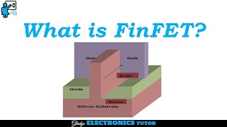
FinFETs, or Fin Field Effect Transistors, represent a step forward in transistor design. Unlike traditional MOSFETs, which have a flat structure, FinFETs are designed in three dimensions. This 3D design allows for better performance, especially in very small technology nodes where traditional MOSFETs struggle due to issues such as leakage current. In short, FinFETs provide a more effective way to manage electrical currents in small circuits, making them essential for modern technology.
Examples & Analogies
Think of FinFETs like a multi-layered cake compared to a flat pie. The multi-layered cake allows for more ingredients and flavors mixed together (representing improved control over electrical properties), while the flat pie, although tasty, has limitations in terms of how many flavors and textures it can accommodate.
Importance of the Chapter
Chapter 2 of 2
🔒 Unlock Audio Chapter
Sign up and enroll to access the full audio experience
Chapter Content
This chapter explores the detailed structure, fabrication process, and operational principles of FinFETs.
Detailed Explanation
In this chapter, we'll delve into the specifics of FinFET technology. We'll discover how these devices are structured, their manufacturing processes, and how they operate. By understanding these elements, you will appreciate why FinFETs are the backbone of modern integrated circuits and how they contribute to advancements in electronic devices. We aim to build a comprehensive understanding of both the theoretical and practical aspects of these transistors.
Examples & Analogies
Imagine learning about a new recipe. First, you find out the ingredients (structure), then how to prepare them (fabrication), and finally how they come together to create a dish (operation). Similarly, this chapter aims to guide you through the essential components of FinFETs step by step.
Key Concepts
-
3D transistor structure: FinFETs possess a vertical long structure that enhances the electrostatic control.
-
Leakage current reduction: Improved gate control helps in minimizing unwanted leakage, thus increasing efficiency.
-
Scalability: FinFETs facilitate scaling in technology nodes down to 7nm and below, making them crucial for modern computing.
Examples & Applications
FinFET technology is implemented in modern CPUs and GPUs, where performance at smaller nodes significantly impacts power efficiency.
In advanced smartphones and laptops, FinFETs help deliver increased battery life while maintaining high computational powers.
Memory Aids
Interactive tools to help you remember key concepts
Rhymes
In the world of chips, FinFET takes the lead, reducing leakages, it fulfills the need.
Stories
Imagine a tall building (the fin) surrounded by multiple balconies (the gate) where people can control activities happening on different floors (sides) at once.
Memory Tools
Think 'LEAP' for FinFET: Leakage, Enhanced performance, and Advanced scalability.
Acronyms
FRESH
FinFETs Reduce Electrical Leakage for Higher performance.
Flash Cards
Glossary
- FinFET
Fin Field Effect Transistor, a type of transistor featuring a 3D fin-shaped channel design.
- MOSFET
Metal-Oxide-Semiconductor Field-Effect Transistor, a traditional type of transistor used in modern electronics.
- DIBL
Drain-Induced Barrier Lowering, a phenomenon where the drain voltage influences the threshold voltage of a transistor.
- Submicron
Referring to technology nodes smaller than one micron, often involving nm-scale semiconductors.
Reference links
Supplementary resources to enhance your learning experience.