
Summary of Key Concepts
Interactive Audio Lesson
Listen to a student-teacher conversation explaining the topic in a relatable way.
Introduction to FinFET Technology
🔒 Unlock Audio Lesson
Sign up and enroll to listen to this audio lesson

Today we're discussing FinFET technology. FinFETs are designed to overcome the limitations of planar MOSFETs. Can anyone tell me what a limitation of planar MOSFETs could be?

They can't really scale down much without performance issues.
Exactly! As we decrease the size, leakage current increases. That's where FinFETs shine with their 3D structure. Let's remember it with the acronym FINE: Fin shape, Improved control, No leakage, Enhanced performance.
Fabrication Process of FinFETs
🔒 Unlock Audio Lesson
Sign up and enroll to listen to this audio lesson

Now, let’s dive into the fabrication process of FinFETs. Can anyone describe the initial steps?

It starts with preparing the substrate!
Right! We begin with a Silicon-on-Insulator wafer. Then, we pattern the fin structures, etch them, and create the gate. It involves sophisticated techniques! Who remembers a key technique used?

EUV lithography?
Correct! Remember that—EUV for Exciting Ultra-High precision! This highlights the complexity and innovation behind FinFET technologies.
Comparison of FinFETs and MOSFETs
🔒 Unlock Audio Lesson
Sign up and enroll to listen to this audio lesson
Let’s compare FinFETs to traditional MOSFETs. What’s one major difference?

FinFETs have a vertical channel, while MOSFETs have a flat one.
Great observation! This geometric difference enhances control. Can anyone tell me how it impacts the performance?
It improves the I_on/I_off ratio and reduces leakage.
Exactly! Better ratios mean enhanced device efficiency. Let’s reinforce this with the mnemonic ‘LEAK’ – Leakage reduction, Enhanced performance, and Acknowledged scalability.
Application and Standards in Technology
🔒 Unlock Audio Lesson
Sign up and enroll to listen to this audio lesson
FinFET technology is the standard in nodes like 7nm and beyond. What companies are utilizing this technology?
Intel and TSMC!
Correct! This shows how crucial FinFETs are in the semiconductor industry. They’ve become fundamental for performance improvements as we reach extreme scaling. As a takeaway, remember ‘SHINE’ – Scalability, High performance, Innovation at nodes ≤ 7nm, Next-gen integration, and Efficiency.
Introduction & Overview
Read summaries of the section's main ideas at different levels of detail.
Quick Overview
Standard
This section highlights the importance of FinFETs in modern semiconductor technology, illustrating their advanced structure, complex fabrication process, and similarities to MOSFETs. FinFETs present significant advantages in performance, scalability, and are standard in advanced technology nodes.
Detailed
Summary of Key Concepts
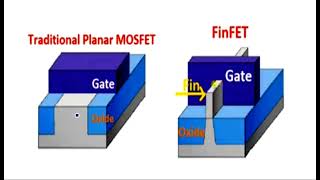
FinFETs, or Fin Field Effect Transistors, represent a significant evolution from traditional planar MOSFETs, particularly in semiconductor manufacturing at deep sub-micron technology nodes. This section encapsulates several key points:
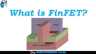
- 3D Structure: FinFETs utilize a 3D fin-shaped channel with multi-gate control that enhances electrostatic performance and minimizes leakage currents, addressing challenges of scaling seen in planar MOSFETs.
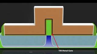
- Complex Fabrication: While FinFET fabrication is more intricate than for traditional MOSFETs, it supports continued scaling down to 7nm, 5nm, and even 3nm nodes. This involves precise processes such as lithography, etching, and conformal deposition to create the necessary structures.
- Operational Characteristics: Operating principles parallel those of MOSFETs but are bolstered by superior electrostatic control, enabling lower off-state leakage and improved current drive capabilities.
- Technological Significance: FinFET technology has become the standard in leading-edge semiconductor manufacturing, adopted by major foundries like Intel, TSMC, and Samsung. Its advantages in performance and scalability validate its prevalence in the industry.
Youtube Videos

Audio Book
Dive deep into the subject with an immersive audiobook experience.
3D Fin-Shaped Channel and Multi-Gate Control
Chapter 1 of 4
🔒 Unlock Audio Chapter
Sign up and enroll to access the full audio experience
Chapter Content
FinFETs use a 3D fin-shaped channel and multi-gate control to enhance performance and reduce leakage.
Detailed Explanation
FinFETs are constructed differently from traditional planar MOSFETs. Instead of having a flat channel, they feature a vertical fin that increases the surface area for electrostatic control. By wrapping the gate around multiple sides of the fin, FinFETs achieve better control over the channel, leading to improved performance and decreased leakage currents. This design contrasts with typical transistors that only have controlling gates on one side.
Examples & Analogies
Imagine trying to control a balloon by only pushing on one side. It’s challenging because the air can equally escape from other sides. Now imagine pushing on all sides of the balloon – you can shape it much better and control it effectively. The multi-gate control in FinFETs functions similarly, allowing for finer control over the electrical flow without unnecessary losses.
Complex Fabrication Compared to Planar MOSFETs
Chapter 2 of 4
🔒 Unlock Audio Chapter
Sign up and enroll to access the full audio experience
Chapter Content
Fabrication is more complex than planar MOSFETs but enables advanced scaling.
Detailed Explanation
Creating FinFETs is technically more challenging than constructing traditional MOSFETs. The process involves intricate steps to form the fin structures and to ensure the gates effectively wrap around these fins. However, this complexity is worthwhile because it allows chip designers to scale down the size of transistors to very small dimensions (like 7nm, 5nm, and even 3nm), which is crucial for modern electronics, making them faster and more efficient.
Examples & Analogies
Think of building a multi-level LEGO structure compared to a simple flat one. While the multi-level design takes more effort to build because you have to ensure everything is balanced and fitting correctly, the final product is more intricate and powerful, allowing for more features in a compact space.
Similarity to MOSFET Operation with Advantages
Chapter 3 of 4
🔒 Unlock Audio Chapter
Sign up and enroll to access the full audio experience
Chapter Content
FinFET operation is similar to MOSFETs but benefits from better electrostatics and drive strength.
Detailed Explanation
While FinFETs follow the same basic operational principles as traditional MOSFETs—such as having different regions like cutoff, linear, and saturation—they excel in performance due to their enhanced electrostatic control. The gate's ability to interact with the channel from multiple sides leads to lower leakage currents and a stronger drive current, which means they can switch on and off more effectively than planar MOSFETs. This enhancement allows for more efficient power use in devices.
Examples & Analogies
Consider switching on a garden hose. If you only partially cover the nozzle, you get a weak spray of water, but if you control the nozzle fully, you have a strong, focused stream. FinFETs effectively manage the flow of current much like fully controlling that hose, providing better performance and efficiency in electronic devices.
Standardization in Advanced CMOS Nodes
Chapter 4 of 4
🔒 Unlock Audio Chapter
Sign up and enroll to access the full audio experience
Chapter Content
These devices are the standard in 7nm, 5nm, and 3nm CMOS nodes.
Detailed Explanation
FinFETs have become the industry standard for cutting-edge semiconductor manufacturing processes at very small scales, namely 7nm, 5nm, and 3nm. This transition is crucial for maintaining the trend of increasing transistor density and performance while keeping power consumption under control. As new technologies emerge, the need for smaller and more efficient transistors becomes paramount for advancements in computing power.
Examples & Analogies
Think about how smartphones have shrunk over the past decade while becoming more powerful. Just as manufacturers had to innovate by using more compact but powerful batteries and processors, the semiconductor industry has adopted FinFET technology to ensure they can create smaller chips that retain their capabilities in a hyper-competitive market.
Key Concepts
-
FinFET Structure: A 3D fin-shaped channel and multi-gate control enhance performance.
-
Fabrication Complexity: The intricate process includes multiple steps like substrate preparation and lithography.
-
Electrostatic Control: Improved control leads to reduced leakage and better drive strength.
-
Industry Standards: FinFETs are the standard technology in cutting-edge semiconductor nodes.
Examples & Applications
FinFETs are used in Intel's 10nm chip architecture to enhance performance over previous generations.
TSMC has adopted FinFET technology for their 7nm and 5nm processes, improving efficiency and scalability.
Memory Aids
Interactive tools to help you remember key concepts
Rhymes
FinFETs are here to stay, No more leaks in play! With multi-gate control, Performance takes its toll!
Stories
Imagine a fish swimming through a tight coral tree - that's like a fin-shaped channel, ensuring it can glide smoothly without losing speed. FinFETs give us that smooth flow in electronics, preventing losses at small sizes!
Memory Tools
To remember the benefits of FinFET: 'SHINE' - Scalability, High performance, Innovation, Next-gen integration, Efficiency.
Acronyms
FINE - Fin shape, Improved control, No leakage, Enhanced performance.
Flash Cards
Glossary
- FinFET
A type of multi-gate transistor technology that enhances control over the channel by utilizing a three-dimensional fin-shaped geometry.
- DIBL
Drain-Induced Barrier Lowering; a phenomenon affecting short-channel devices that negatively impacts performance.
- Gate Dielectric
An insulating layer, typically high-k material, that separates the gate from the channel in a transistor.
- SOI
Silicon-on-Insulator; a semiconductor fabrication technique used to improve performance and reduce parasitic effects.
Reference links
Supplementary resources to enhance your learning experience.