
Spacer Formation and Source/Drain Implantation
Interactive Audio Lesson
Listen to a student-teacher conversation explaining the topic in a relatable way.
Introduction to Spacer Formation
🔒 Unlock Audio Lesson
Sign up and enroll to listen to this audio lesson

Today we will talk about spacer formation in FinFETs. Can anyone tell me what a spacer is and why we need it?

I think spacers are materials added during the fabrication to separate different components, right?
Exactly! Spacers are important for electrical isolation. They keep the gate from interfering with the source and drain regions. They can be made of materials like silicon dioxide or silicon nitride.

So, do spacers also help maintain the structure of the fin?
Great observation! Yes, they provide structural support, helping to ensure that the dimensions stay true during fabrication. Let’s remember: Spacers = Structural support + Isolation.
Source and Drain Implantation
🔒 Unlock Audio Lesson
Sign up and enroll to listen to this audio lesson

Now, let’s move to source and drain implantation. Why do you think doping these regions is critical?

Is it to enhance their conductivity?
Yes! The source and drain must be heavily doped for efficient charge transport. The doping concentration directly impacts the device's performance.

What happens if the doping is not controlled?
Good question! If doping isn't controlled, it can lead to higher leakage currents and reduced current drive capability. Always remember: Doping = Performance.
Integration of Spacer and Doping Processes
🔒 Unlock Audio Lesson
Sign up and enroll to listen to this audio lesson
How do you think spacer formation and source/drain doping work together in FinFET fabrication?
They happen in sequence, right? Spacers create separation, which allows for accurate doping?
Exactly! The spacers ensure that we have a defined area for doping. This process sequence prevents overlap, maintaining device integrity and performance.
And since they're both crucial, does that mean they have to be done with high precision?
Spot on! Precision at this stage is key for device reliability as we push towards smaller nodes.
Introduction & Overview
Read summaries of the section's main ideas at different levels of detail.
Quick Overview
Standard
The section discusses how spacers are formed beside the gate and how the source and drain regions are heavily doped to ensure efficient conductivity. The significance of these processes in enhancing the performance of FinFETs is emphasized.
Detailed
Spacer Formation and Source/Drain Implantation
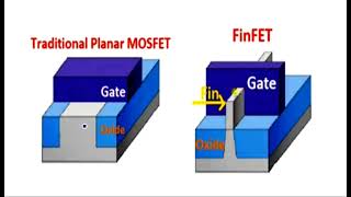
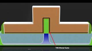
In the fabrication of FinFETs, spacer formation and source/drain implantation are essential steps that contribute significantly to the overall device performance. After the gate stack formation, spacers are added on either side of the gate. These spacers, typically made from materials like silicon dioxide or silicon nitride, serve multiple purposes:
- Electrical Isolation: They help in electrically isolating the gate from the source and drain regions.
- Structural Integrity: Spacers provide structural support to the fin and the gate, ensuring that the dimensions remain stable during subsequent manufacturing steps.
Following spacer formation, the source and drain regions, located on either side of the fin, need to be heavily doped. This doping process enhances the conductivity of these regions, enabling efficient charge transport and overall device functionality. The careful control of the doping concentration is crucial, as it directly influences the electrical characteristics of the FinFET, such as current drive capability and leakage current.
In summary, the processes of spacer formation and source/drain implantation are crucial for optimizing the performance and reliability of FinFET devices, particularly as technology scales down to smaller nodes.
Youtube Videos


Audio Book
Dive deep into the subject with an immersive audiobook experience.
Spacer Formation
Chapter 1 of 2
🔒 Unlock Audio Chapter
Sign up and enroll to access the full audio experience
Chapter Content
○ Add spacers beside the gate.
Detailed Explanation
Spacer formation is a crucial step in the fabrication of FinFETs. After the gate stack has been created around the fins, spacers, which are thin layers of insulating material, are added on either side of the gate. This is done to help define the active areas for the source and drain regions. The spacers ensure that these regions are well-separated and properly aligned with the gate, preventing any unwanted electrical interference.
Examples & Analogies
Think of spacers like the barriers used in a parking lot. Just like barriers help to mark where each car should park and keep them from bumping into each other, spacers help to define where the source and drain are supposed to be, ensuring they are correctly positioned relative to the gate.
Source/Drain Implantation
Chapter 2 of 2
🔒 Unlock Audio Chapter
Sign up and enroll to access the full audio experience
Chapter Content
○ Dope source and drain regions heavily for conductivity.
Detailed Explanation
Once the spacers are in place, the next step is the implantation of impurities, or 'doping,' in the source and drain regions of the FinFET. This is done to increase the conductivity of these regions, allowing them to effectively inject and extract charge carriers (electrons or holes) when the device is in operation. The doping process involves introducing specific elements, like phosphorus or boron, into the silicon structure. The concentration and type of dopant can greatly affect the performance of the FinFET.
Examples & Analogies
Imagine adding flavoring to a dish. Just as you would sprinkle in salt or spices to enhance the taste and make it more enjoyable, doping the source and drain regions enhances their ability to conduct electricity, improving how the FinFET performs in a circuit.
Key Concepts
-
Spacer Formation: Essential for electrical isolation and provides structural support.
-
Source/Drain Implantation: Heavily doping these regions enhances conductivity.
-
Process Integration: The sequencing and precision of spacer and doping processes affect device integrity.
Examples & Applications
When fabricating a FinFET, silicon dioxide is commonly used as a spacer material to ensure isolation between the gate and the source/drain.
In FinFETs used in modern processors, the doping levels of source/drain regions may be increased to improve performance and reduce leakage currents.
Memory Aids
Interactive tools to help you remember key concepts
Rhymes
Spacers hold the gate in place, Keeping currents from the race.
Stories
Imagine a bustling city where towers (spacers) hold the skyline (gate) up, ensuring that private homes (source/drain) don’t interfere with public transport (electricity).
Memory Tools
To recall spacer roles: IS (Isolation and Support = Spacer).
Acronyms
DOPED (Doping Optimizes Performance in Electrical Devices).
Flash Cards
Glossary
- Spacer
Material added during FinFET fabrication that provides electrical isolation and structural support.
- Doping
The process of adding impurities to a semiconductor to change its electrical properties.
- Source/Drain Regions
Heavily doped areas adjacent to the channel of a FinFET that allow charge carriers to enter and exit.
Reference links
Supplementary resources to enhance your learning experience.