
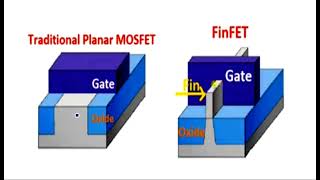
Gate Stack Formation
Interactive Audio Lesson
Listen to a student-teacher conversation explaining the topic in a relatable way.
Introduction to Gate Stack Formation
🔒 Unlock Audio Lesson
Sign up and enroll to listen to this audio lesson

Today, we're going to dive into gate stack formation. Can anyone tell me why this process is so crucial in FinFETs?

Is it because it controls the electrical characteristics of the transistor?
Yes, that's right! The gate stack is essential for controlling the channel. Now, we typically use high-κ dielectrics. Who can explain what high-κ means?

It refers to materials with a high dielectric constant, right?
Exactly! High-κ dielectrics allow for better electrostatic control, which leads to lower leakage. Let's remember that with the acronym 'H-K' for high-κ.

What specific materials do we use for the gate?
Good question! A common choice is HfO₂, which is Hafnium Oxide. It plays a significant role in gate stack performance.

How is the gate applied to the fin?
We use conformal deposition, ensuring that the gate material wraps uniformly around the fin. This configuration is crucial for maximizing gate control.
To summarize, gate stack formation is vital for effective FinFET function, relying on high-κ dielectrics and uniform wrapping to enhance device performance.
Impact of Gate Stack on Device Performance
🔒 Unlock Audio Lesson
Sign up and enroll to listen to this audio lesson

Let's discuss the impact of gate stack formation on FinFET performance. Why is it important to achieve a good gate stack?
To reduce leakage currents and improve the off-state performance.
Correct! By minimizing leakage, we enhance the overall energy efficiency. Can anyone provide an example of how this impacts real-world applications?
In mobile devices, battery life would improve due to reduced power consumption.
Exactly! Less leakage extends battery life. Now, let's remember this with the motto 'Less Leakage, More Life' for FinFET devices. What else contributes to gate stack efficiency?
The uniformity of the gate material around the fin is crucial.
Absolutely! Uniform gate coverage ensures consistent electrical performance across the fin structure.
In summary, an effective gate stack formation reduces leakage, boosts performance, and is essential for practical applications like your smartphones.
Introduction & Overview
Read summaries of the section's main ideas at different levels of detail.
Quick Overview
Standard
This section details the process of gate stack formation in FinFET devices, highlighting the materials used, the significance of high-κ dielectrics, and their impact on device performance. The formation process is crucial for ensuring effective gate control and minimizing leakage current.
Detailed
Gate Stack Formation
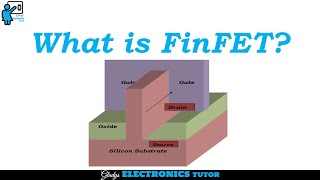
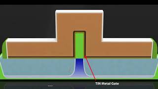
The gate stack formation is a critical stage in FinFET fabrication that involves depositing high-κ dielectric materials such as HfO₂ and metal to create a conductive gate that envelops the fin structure. This multi-layer configuration allows for enhanced electrostatic control over the channel formed by the fin, which is essential for reducing leakage and improving overall device performance. The conformal deposition technique ensures that the gate material uniformly wraps around the fin, maximizing the effective gate area. This section emphasizes the importance of gate stack formation as a key step in achieving the desired electrical characteristics and operational efficiency of FinFET devices.
Youtube Videos

Audio Book
Dive deep into the subject with an immersive audiobook experience.
Introduction to Gate Stack Formation
Chapter 1 of 2
🔒 Unlock Audio Chapter
Sign up and enroll to access the full audio experience
Chapter Content
Gate Stack Formation
- Deposit high-κ dielectric (e.g., HfO₂) and metal gate material.
- Gate wraps around the fin using conformal deposition.
Detailed Explanation
The gate stack formation is a critical step in creating FinFETs. It involves two main actions: first, depositing a high-k dielectric material, which is an insulator that helps create a strong electrical field when voltage is applied. HfO₂ (Hafnium Oxide) is commonly used for this purpose due to its excellent properties. Second, a metal gate material is deposited over this dielectric. The process of deposition must be done in a way that the gate completely wraps around the fin structure. This wrapping is achieved through a technique known as conformal deposition, which ensures that the material coats even the most intricate parts of the fin uniformly.
Examples & Analogies
Think of wrapping a present with gift wrap. You want to make sure the wrapping paper covers every part of the box without any gaps. If you miss a corner, the gift might not look as appealing, and the corners might be exposed. Similarly, in gate stack formation, the wrapping represents how the gate material must be applied uniformly around the fin to ensure that it functions effectively without any weak points.
Role of High-κ Dielectric
Chapter 2 of 2
🔒 Unlock Audio Chapter
Sign up and enroll to access the full audio experience
Chapter Content
High-κ dielectric materials enhance the gate control over the channel, leading to better performance.
Detailed Explanation
The use of high-κ dielectric materials is crucial in FinFET technology because they allow for stronger electric fields without needing an excessively thick layer of material. This leads to better control over the channel between the source and drain. With enhanced gate control, there is reduced leakage current and improved device performance. In addition, these materials enable the FinFET devices to operate effectively at smaller scales, which is important for modern semiconductor manufacturing.
Examples & Analogies
Consider a water faucet: if the faucet is small, you can only control a small stream of water. If it’s wider (providing a stronger flow of water, or high-κ dielectric), you can better manage how much water comes out without splashing everywhere. This illustrates how high-κ materials improve control and efficiency in semiconductor devices, just as a better faucet allows for more controlled water flow.
Key Concepts
-
Gate Stack: The structure formed by dielectric materials and the metal gate, crucial for controlling the FinFET channel.
-
High-κ Dielectrics: Materials with a high dielectric constant that enhance control over the transistor's electrostatics.
-
Conformal Deposition: A method used to apply gate materials uniformly around the fin structure.
Examples & Applications
The use of HfO₂ as a high-κ dielectric improves the electrostatic control of the channel, leading to enhanced performance in high-speed applications.
Conformal deposition ensures that the metal gate wraps around the fin, maximizing the effective gate area and minimizing leakage.
Memory Aids
Interactive tools to help you remember key concepts
Rhymes
With high-κ the gates perform well; lower leakage, hear the bell!
Stories
Imagine a tiny fin, surrounded by a cape. The cape is the high-κ gate, providing control without escape.
Memory Tools
Remember 'G-H-K', for Gate, High-κ, and Control.
Acronyms
H-K for High-κ
Higher capacitance
for control!
Flash Cards
Glossary
- Gate Stack
The combination of the gate electrode and dielectric material in a transistor that controls the channel.
- Highκ Dielectric
A dielectric material with a high relative permittivity, used to enhance gate capacitance and control in transistors.
- Conformal Deposition
A deposition technique that ensures uniform coating of the gate material around complex surfaces like fins.
Reference links
Supplementary resources to enhance your learning experience.