
Fin Patterning and Etching
Interactive Audio Lesson
Listen to a student-teacher conversation explaining the topic in a relatable way.
Introduction to Fin Patterning
🔒 Unlock Audio Lesson
Sign up and enroll to listen to this audio lesson

Today, we are diving into the initial stages of FinFET fabrication, focusing on fin patterning. Can anyone explain why patterning is crucial in this process?

It defines the dimensions of the fins, right? The size affects how well the transistor performs.
Exactly! The dimensions affect electrostatic control. We use advanced lithography techniques such as EUV and DUV. Who can recall what EUV stands for?

Extreme Ultraviolet, I remember that!
Great job! Now, let’s discuss the significance of having precise dimensions for the fins. Thinner fins lead to better control over the channel. Why do you think that is?

Because it allows for a stronger electrostatic control, reducing leakage currents?
Absolutely right! To summarize, fin patterning is critical to defining the performance characteristics of FinFETs, influencing both drive current and leakage.
Etching Process in FinFETs
🔒 Unlock Audio Lesson
Sign up and enroll to listen to this audio lesson

Now let’s transition to the etching aspect of the fabrication process. Why is etching necessary after lithography?

It's how we actually create the fins from the silicon wafer!
Correct! Etching selectively removes silicon from areas not protected by the photoresist layer. What might happen if etching isn't precise?
The fins could end up uneven, which might degrade the device performance?
Exactly! Uneven fins would lead to inconsistencies in electrostatic control and could increase leakage. In summary, successful etching ensures that the fins are uniform and appropriately sized for optimal FinFET performance.
Introduction & Overview
Read summaries of the section's main ideas at different levels of detail.
Quick Overview
Standard
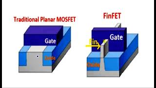
FinFETs require precise fabrication techniques due to their complex 3D structure. Fin patterning and etching are crucial steps in defining the fins, utilizing advanced lithography methods to achieve the desired dimensions necessary for effective performance in semiconductor applications.
Detailed
Fin Patterning and Etching in FinFET Fabrication
FinFETs, or Fin Field Effect Transistors, are an evolution in semiconductor technology designed to overcome the limitations of traditional planar transistors, particularly at sub-micron scales. A key step in the FinFET fabrication process is fin patterning and etching, which involves several critical processes.
- Lithography: Advanced lithography techniques, such as Extreme Ultraviolet Lithography (EUV) or Deep Ultraviolet Lithography (DUV), are employed to precisely define narrow fin structures. This step is crucial because the dimensions of the fins directly impact the electrostatic control and overall performance of the FinFET.
- Etching: Following lithography, etching processes are used to carve the thin, vertical fins into the silicon substrate. This involves selective removal of silicon from the areas not protected by the photoresist, allowing for the creation of the tall, narrow fins that will form the channel of the FinFET.
The significance of fin patterning and etching cannot be understated, as these processes lay the groundwork for the electrical characteristics of the fins, ultimately determining the device's performance in terms of drive current, leakage, and subthreshold slope. High precision in these steps is essential for achieving the desired fin dimensions, thereby enhancing device scalability into future technology nodes.
Youtube Videos

Audio Book
Dive deep into the subject with an immersive audiobook experience.
Overview of Fin Patterning and Etching
Chapter 1 of 2
🔒 Unlock Audio Chapter
Sign up and enroll to access the full audio experience
Chapter Content
Use advanced lithography (EUV/DUV) to define narrow fin structures.
Detailed Explanation
In this step of FinFET fabrication, advanced lithography techniques such as Extreme Ultraviolet (EUV) or Deep Ultraviolet (DUV) are utilized. The purpose of this process is to create precise patterns that define the narrow structures of the fins, which are critical for the performance of the FinFET. These techniques use light to expose a photoresist material, allowing for intricate designs that dictate where the fins will be subsequently etched out.
Examples & Analogies
Consider the process like creating a stencil for painting. Just as a painter would use a finely designed stencil to control the shape of the paint and ensure it lands exactly where desired, lithography works to ensure the silicon fins are shaped accurately for optimal electronic performance.
Etching Process
Chapter 2 of 2
🔒 Unlock Audio Chapter
Sign up and enroll to access the full audio experience
Chapter Content
Etch silicon to form tall, thin fins.
Detailed Explanation
Once the patterns have been defined on the substrate using lithography, the next step is etching the silicon. This involves using various chemicals or plasma to remove silicon from areas not protected by the photoresist, thereby sculpting the fins into tall, thin structures. This is crucial because the dimensions of the fins significantly impact the electrical properties of the FinFET, affecting how well it can control the flow of current and minimize leakage.
Examples & Analogies
Think of etching like carving a sculpture from a block of marble. Only the parts of the marble that are meant to remain will be unscathed, while the unwanted parts are chiseled away. Similarly, etching removes excess silicon to leave behind precisely shaped fins, which will form the core of the transistor.
Key Concepts
-
Fin Patterning: A defining process in FinFET fabrication that uses lithography to form the fin structures.
-
Etching: A process that carves the fins into the silicon substrate after lithography is complete.
Examples & Applications
EUV lithography is utilized to achieve the fine dimensions required for FinFETs in modern semiconductor technology.
Etching creates tall, thin fins essential for enhancing electrostatic control in FinFETs.
Memory Aids
Interactive tools to help you remember key concepts
Rhymes
Etch and sketch, define it right, fins so narrow, a transistor's light.
Stories
Imagine artists etching fine lines into a stone, shaping the perfect silhouette just like engineers shape fins from silicon.
Memory Tools
LEAF - Lithography, Etching, Accurate Fins.
Acronyms
FINE - Fin Inducing Nanofabrication Effects.
Flash Cards
Glossary
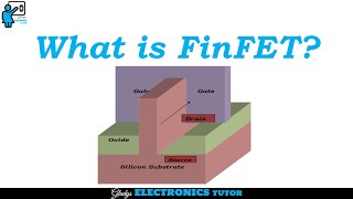
- FinFET
A type of 3D transistor characterized by a thin, vertical silicon fin that forms the channel.
- Lithography
A process used to pattern parts of a thin film or the bulk of a substrate.
- EUV Lithography
Extreme Ultraviolet Lithography, a technology used in semiconductor manufacturing to create extremely small features.
- Etching
A fabrication process used to remove layers from a surface, typically to create patterns on silicate wafers.
- Photoresist
A light-sensitive material used to form a patterned coating on a surface.
Reference links
Supplementary resources to enhance your learning experience.