
FinFET Fabrication Process (Simplified)
Interactive Audio Lesson
Listen to a student-teacher conversation explaining the topic in a relatable way.
Substrate Preparation
🔒 Unlock Audio Lesson
Sign up and enroll to listen to this audio lesson

Let's start by discussing substrate preparation. FinFETs require a strong base, which can be either a Silicon-on-Insulator or a bulk silicon wafer. Why do you think the choice of substrate material is crucial for FinFETs?

I think it's important because it might affect the electrical properties of the FinFET.
Exactly! The substrate provides the foundation for the fin structure and influences the overall device performance. Remember the acronym *SBS* for Substrate: Base for Structure.

What’s the difference between SOI and bulk silicon wafers?
Great question! SOI wafers reduce parasitic capacitance and enhance performance, while bulk silicon is often easier to work with for larger devices. Any further questions on substrates?

No, I get it now!
Fin Patterning and Etching
🔒 Unlock Audio Lesson
Sign up and enroll to listen to this audio lesson

Moving on to fin patterning and etching, what role do you think lithography plays in this process?

Is it used to create the patterns for the fins?
Yes! We use advanced techniques like EUV and DUV lithography to define the narrow fin structures accurately. Remember *FINE*: Fin Identification Needs Etching.
What happens if the fins are not properly etched?
If not etched correctly, the fins could be too thick or too short, which would impact device performance significantly. This is why this step is critical!
Gate Stack Formation
🔒 Unlock Audio Lesson
Sign up and enroll to listen to this audio lesson
Now, let’s talk about gate stack formation. What materials do we typically use for the gate dielectric?
I believe high-κ materials like HfO₂ are used?
Correct! These materials help improve electrostatic control over the channel. We aim for a wrap-around gate design – that’s why memory aids like *GATE* - Gate And Top Engagement are useful!
How does this wrapping improve performance?
Wrapping reduces leakage currents and enhances drive strength because the gate's influence covers more of the channel. Any more questions?
Spacer Formation and Source/Drain Implantation
🔒 Unlock Audio Lesson
Sign up and enroll to listen to this audio lesson
Next, let’s describe spacer formation. Why do you think spacers are necessary during the fabrication process?
Wouldn't they provide stability for the gate?
Exactly! They help maintain the structure of the device. This leads us to the source and drain implantation, where we heavily dope regions for conductivity. Remember *SSD*: Spatial Stability during Doping.
What happens if the doping concentration is incorrect?
Good question! Too low would result in poor conductivity, while too high might lead to leakage. Balance is key!
Silicidation and Interconnects
🔒 Unlock Audio Lesson
Sign up and enroll to listen to this audio lesson
Lastly, let's discuss silicidation and interconnects. Why do we create low-resistance contacts at this stage?
To ensure efficient electrical connectivity?
Precisely! This step is vital for overall device performance. Think of the acronym *CONE*: Contacts Need Effective connection. What about interconnects?
They must connect multiple device elements?
Exactly. This final wiring ensures that all parts of the device can function together seamlessly.
Introduction & Overview
Read summaries of the section's main ideas at different levels of detail.
Quick Overview
Standard
This section outlines the simplified fabrication process of FinFETs, highlighting critical steps such as substrate preparation, fin patterning and etching, gate stack formation, and the importance of advanced techniques like EUV lithography for accuracy and scalability in modern semiconductor manufacturing.
Detailed
FinFET Fabrication Process (Simplified)
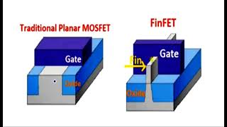
FinFETs require an intricate fabrication process that distinguishes them from traditional planar MOSFETs. The necessary steps are aimed at creating the unique structures essential for FinFET operation:
- Substrate Preparation: FinFETs start with either a Silicon-on-Insulator (SOI) wafer or a bulk silicon wafer, providing a foundation for further processing.
- Fin Patterning and Etching: Advanced lithography techniques, including Extreme Ultraviolet (EUV) and Deep Ultraviolet (DUV) lithography, are employed to define the narrow fin structures necessary for the transistor channel. This is followed by etching processes to form tall, thin silicon fins.
- Gate Stack Formation: A high-κ dielectric layer, such as Hafnium Dioxide (HfO₂), is deposited along with a metal gate material. The goal is to ensure that the gate can effectively wrap around the fins through conformal deposition techniques.
- Spacer Formation and Source/Drain Implantation: Spacers are added beside the gate to enhance the device's structure. Heavily doped regions are then implanted to form the source and drain, facilitating conductivity.
- Silicidation and Contacts: Low-resistance contacts are created using metal silicide, which is essential for efficient electrical connectivity.
- Interconnects: Finally, metal layers are created for wiring through damascene or dual-damascene processes. Advanced manufacturing nodes benefit from self-aligned patterning and gate-last processing, which improve accuracy and reduce device variation.
This comprehensive approach allows FinFETs to be fabricated with precision, addressing performance and scalability in the field of semiconductor devices.
Youtube Videos

Audio Book
Dive deep into the subject with an immersive audiobook experience.
Substrate Preparation
Chapter 1 of 7
🔒 Unlock Audio Chapter
Sign up and enroll to access the full audio experience
Chapter Content
- Substrate Preparation
○ Start with a Silicon-on-Insulator (SOI) or bulk silicon wafer.
Detailed Explanation
The first step in the FinFET fabrication process involves preparing the substrate, which is the base material on which the device is built. There are two common types of substrates: Silicon-on-Insulator (SOI) and bulk silicon wafers. SOI wafers consist of a thin layer of silicon on top of an insulating layer (often made of silicon dioxide), while bulk silicon wafers are just a single layer of silicon. The choice of substrate affects the electrical properties and performance of the FinFET devices. Using SOI can reduce parasitic capacitance and improve performance.
Examples & Analogies
Think of the substrate like the foundation of a house. Just as a strong foundation is necessary for a stable and durable house, the right substrate is critical for ensuring that the FinFET operates correctly and efficiently.
Fin Patterning and Etching
Chapter 2 of 7
🔒 Unlock Audio Chapter
Sign up and enroll to access the full audio experience
Chapter Content
- Fin Patterning and Etching
○ Use advanced lithography (EUV/DUV) to define narrow fin structures.
○ Etch silicon to form tall, thin fins.
Detailed Explanation
In this step, advanced lithography techniques such as Extreme Ultraviolet (EUV) or Deep Ultraviolet (DUV) are employed to precisely define the patterns of the fins on the silicon substrate. Lithography is similar to taking a photograph where the pattern is projected onto the surface. After the pattern is created, a process called etching is used to remove unwanted silicon, resulting in tall and thin silicon fins that will serve as the channels for the FinFET. The dimensions of these fins are crucial as they directly influence the performance characteristics of the device.
Examples & Analogies
Imagine using a stencil to create intricate cookie shapes. First, you lay the stencil over the dough (lithography), then cut the dough (etching) to get the final cookie shapes. Just like the cookie shapes determine what you can bake, the fin shapes influence the electrical characteristics of the FinFET.
Gate Stack Formation
Chapter 3 of 7
🔒 Unlock Audio Chapter
Sign up and enroll to access the full audio experience
Chapter Content
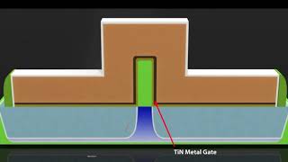
- Gate Stack Formation
○ Deposit high-κ dielectric (e.g., HfO₂) and metal gate material.
○ Gate wraps around the fin using conformal deposition.
Detailed Explanation
This step involves creating the gate stack, which includes depositing a layer of high-κ (high dielectric constant) material such as Hafnium Dioxide (HfO₂) followed by a metal gate material. High-κ materials are important because they enable better control over the channel, reducing leakage currents. A technique called conformal deposition is used to ensure that the gate material coats all sides of the fin evenly. This wrapping of the gate around the fin is crucial for maximizing the electrostatic control over the channel.
Examples & Analogies
Consider how a parent may wrap their arms around a child for protection. The gate material acts like the parent's arms, providing support and control over the fin, ensuring the child's safety and well-being. In this case, the safety of the fin (device) is ensured by the gate's efficient control.
Spacer Formation and Source/Drain Implantation
Chapter 4 of 7
🔒 Unlock Audio Chapter
Sign up and enroll to access the full audio experience
Chapter Content
- Spacer Formation and Source/Drain Implantation
○ Add spacers beside the gate.
○ Dope source and drain regions heavily for conductivity.
Detailed Explanation
In this step, spacers are added beside the gate. These spacers help define the boundaries of the gate region and improve the electrical characteristics of the FinFET. Following this, the source and drain regions are heavily doped with impurities to enhance their electrical conductivity. This means adding atoms that will increase the number of charge carriers (electrons or holes) in these regions, allowing them to efficiently inject and collect current.
Examples & Analogies
Think of spacers like the padding around a box that helps keep items secure inside. Just as padding prevents items from moving around and getting damaged, spacers help maintain the integrity of the device's structure while simultaneously enhancing performance by allowing current to flow effectively.
Silicidation and Contacts
Chapter 5 of 7
🔒 Unlock Audio Chapter
Sign up and enroll to access the full audio experience
Chapter Content
- Silicidation and Contacts
○ Form low-resistance contacts using metal silicide.
Detailed Explanation
This step focuses on forming low-resistance electrical contacts at the sources and drains of the FinFET. This is done through a process called silicidation, where a metal is reacted with silicon to form a silicide, which has a much lower resistance than silicon alone. Low-resistance contacts are essential for ensuring that the FinFET can operate efficiently and maintain performance as current levels increase.
Examples & Analogies
Imagine a busy highway where traffic flows smoothly versus a poorly designed intersection that slows traffic down. The low-resistance contacts act like the smooth highway, facilitating efficient current flow and preventing bottlenecks in the device’s operation.
Interconnects
Chapter 6 of 7
🔒 Unlock Audio Chapter
Sign up and enroll to access the full audio experience
Chapter Content
- Interconnects
○ Create metal layers for wiring using damascene or dual-damascene processes.
Detailed Explanation
In this final step of the fabrication process, metal interconnects are created to connect various components of the FinFET. Techniques like damascene or dual-damascene processes are used to form these wiring layers. These processes ensure that the interconnects are both efficient and reliable, providing necessary pathways for electrical signals and power between different parts of the circuit. Proper interconnect architecture is crucial for the overall speed and functionality of the chip.
Examples & Analogies
Think of interconnects like the wiring in a house. Just as electrical wires connect different rooms and appliances, allowing for the flow of electricity, interconnects link different components of the chip together, ensuring that signals and power can reach where they are needed.
Advanced Techniques
Chapter 7 of 7
🔒 Unlock Audio Chapter
Sign up and enroll to access the full audio experience
Chapter Content
Advanced nodes may use self-aligned patterning, gate-last processing, or EUV lithography to improve accuracy and reduce variation.
Detailed Explanation
As technology advances, more sophisticated techniques may be employed to improve the accuracy and efficiency of the FinFET fabrication process. Self-aligned patterning allows features to be aligned automatically during manufacturing, which reduces alignment errors. Gate-last processing is another advanced technique that optimizes the gate formation process. EUV lithography offers improvements in resolving power, enabling the creation of smaller and more intricate structures. These techniques are important for maintaining performance and yield as transistors shrink to smaller technology nodes.
Examples & Analogies
Consider how technological advancements in photography have allowed for sharper and clearer images. Just like modern cameras use advanced techniques to capture more detailed pictures, advanced fabrication methodologies enable the creation of more precise and effective FinFET devices, leading to better performance.
Key Concepts
-
Substrate Preparation: The choice of substrate, such as SOI or bulk silicon, is critical for performance and scalability.
-
Fin Patterning and Etching: Advanced lithography is crucial for defining the fin structures.
-
Gate Stack Formation: High-κ dielectrics are essential for effective electrostatic control.
-
Spacer Formation and Source/Drain Implantation: Spacers stabilize the structure while doping enhances conductivity.
-
Silicidation and Interconnects: These steps ensure efficient electrical performance of the device.
Examples & Applications
Using SOI wafers can significantly diminish noise in high-performance applications.
Advanced lithography techniques reduce variations in fin dimensions, improving yield in production.
Memory Aids
Interactive tools to help you remember key concepts
Rhymes
For fins that are tidy, they start on the side, / Patterns in litho make performance glide.
Stories
Imagine building a tower but first needing a solid foundation. The substrate is that foundation that ensures everything built on it is strong and stable, just like a FinFET's performance.
Memory Tools
Remember SFGIS: Substrate, Fin, Gate, Interconnects, Source/Drain for the fabrication process steps!
Acronyms
Use 'ADS' - Advanced Design Steps to remember the critical techniques like EUV and DUV in lithography.
Flash Cards
Glossary
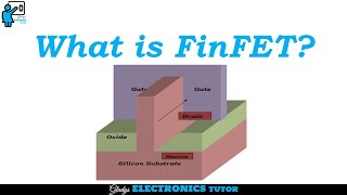
- FinFET
A Fin Field Effect Transistor that utilizes a 3D fin structure for improved performance.
- SilicononInsulator (SOI)
A semiconductor fabrication technique that uses a layered structure for improved performance.
- EUV Lithography
A cutting-edge technology for photolithography, using extreme ultraviolet light to produce very fine patterns.
- Doping
The process of adding impurities to semiconductor materials to change their electrical properties.
- Silicidation
A process of forming low-resistance metal silicide contacts in semiconductor devices.
Reference links
Supplementary resources to enhance your learning experience.