
2D Material FETs
Interactive Audio Lesson
Listen to a student-teacher conversation explaining the topic in a relatable way.
Introduction to 2D Materials
🔒 Unlock Audio Lesson
Sign up and enroll to listen to this audio lesson

Today, we're diving into 2D Material FETs, which use materials like MoS₂ and graphene. Can anyone tell me what a 2D material is?

Is it a material that is only a few atoms thick?
Exactly! Atomic thickness allows these materials to provide exceptional gate control. Remember the acronym GATE: Gate control, Atomic thickness, Tuning performance, Excellent integration potential.

So, can these be used for different electronic devices?
Great question! They are indeed versatile, making them suitable for many applications, such as low-power devices.

Why is that important?
Low power means less energy consumption and heat generation, which is crucial in modern computing!
To recap: 2D materials enhance control, reduce power consumption, and improve device integration.
Advantages of 2D Material FETs
🔒 Unlock Audio Lesson
Sign up and enroll to listen to this audio lesson

Let’s explore the advantages of using 2D materials in FETs. What do you think makes them better than traditional materials?

Do they have better electrical properties?
Yes, 2D materials often exhibit higher carrier mobility. This leads to faster switching times. Think SPEED: Superior performance, Enhanced efficiency, Exceptional density, and Detail-oriented designs.
What about their scalability?
Great point! Because they are so thin, these FETs can scale down effectively without the same limitations as bulk materials, allowing for continued innovation.
Remember, 2D Material FETs provide enhanced performance and integration potential at the nanoscale!
Real-World Applications
🔒 Unlock Audio Lesson
Sign up and enroll to listen to this audio lesson
Now, let’s look at how these 2D Material FETs are applied in real-world scenarios. Can anyone think of industries that could benefit from this technology?
I think smartphones! They want to be small and powerful.
Exactly! Think about the GATE again - Gate control, Atomic thickness, Tuning performance. It’s perfect for devices that require compact design and high efficiency.
What about computers?
Definitely! 2D Material FETs could enable faster processors that consume less power, making it attractive for both laptops and data centers.
To summarize, the integration of 2D material technology in various electronic devices enhances their speed and efficiency!
Introduction & Overview
Read summaries of the section's main ideas at different levels of detail.
Quick Overview
Standard
This section covers the significance of 2D Material FETs in modern semiconductor technology. It highlights how these transistors, using materials like MoS₂, WS₂, and graphene, provide exceptional electrostatic control and are suitable for ultra-scaled channels, thereby contributing to the ongoing advances in device miniaturization.
Detailed
2D Material FETs
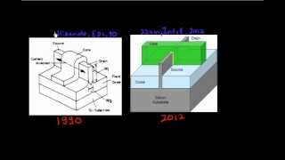
2D Material FETs represent a significant advancement in the realm of semiconductor devices. These transistors utilize materials such as Molybdenum disulfide (MoS₂), Tungsten disulfide (WS₂), and graphene, which have unique properties that make them ideal for ultra-thin and efficient electronic applications.
Key Points:
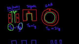
- Composition: The semiconductor channel is composed of 2D materials, characterized by their atomic thickness, which provides an unprecedented level of gate control over the channel.
- Performance: 2D Material FETs are capable of operating at very low voltages while maintaining high performance, making them attractive for low-power applications.
- Integration Potential: Their thin nature allows for high-density integration in devices, facilitating advancements in nanoelectronics over traditional transistor technologies. They promise to enhance the performance of various applications, from consumer electronics to high-performance computing.
As the semiconductor industry grapples with the limitations of existing technologies, 2D Material FETs offer a compelling glimpse into the future of electronic devices, combining simplicity in design with sophisticated functionality.
Youtube Videos

Audio Book
Dive deep into the subject with an immersive audiobook experience.
Introduction to 2D Material FETs
Chapter 1 of 3
🔒 Unlock Audio Chapter
Sign up and enroll to access the full audio experience
Chapter Content
● Channels made from materials like MoS₂, WS₂, graphene.
● Ultra-thin body offers excellent gate control.
Detailed Explanation
2D Material FETs are a type of field-effect transistor that utilizes materials which are only a few atoms thick, such as molybdenum disulfide (MoS₂), tungsten disulfide (WS₂), and graphene. These materials possess unique electrical properties, allowing them to effectively control the flow of electricity with a minimal thickness—often one or two atoms thick. This characteristic, known as an ultra-thin body, leads to more effective gate control compared to traditional materials, making these devices potentially more efficient and faster.
Examples & Analogies
Imagine a water faucet where the thickness of the pipe affects water flow. A thinner pipe means better control over the water, allowing for precise adjustments. Similarly, the ultra-thin body of 2D Material FETs offers exceptional control over electrical current, making them ideal for advanced electronic applications.
Benefits of 2D Material FETs
Chapter 2 of 3
🔒 Unlock Audio Chapter
Sign up and enroll to access the full audio experience
Chapter Content
● Excellent electrostatics due to the thin channel design.
● Potential for integration in flexible electronics and nanoscale devices.
Detailed Explanation
The great advantage of using 2D materials in FETs lies in their exceptional electrostatic control stemming from their thin architecture. This enhances the device's ability to switch on and off efficiently, which is crucial for performance in electronic applications. Additionally, the flexibility of 2D materials opens doors for new uses in technology, such as flexible electronics that can bend and conform to various shapes and surfaces, as well as in the miniaturization of devices, allowing for increasingly dense integration of components.
Examples & Analogies
Consider how a piece of thin, flexible plastic can easily be twisted and turned compared to a rigid metal sheet. Just like the plastic, 2D Material FETs can be adapted to innovative shapes and applications, making electronics lighter and more versatile.
Applications of 2D Material FETs
Chapter 3 of 3
🔒 Unlock Audio Chapter
Sign up and enroll to access the full audio experience
Chapter Content
● Ideal for use in high-performance, low-power devices.
● Can potentially enhance the capabilities of logic circuits.
Detailed Explanation
2D Material FETs show great promise for applications requiring high performance while minimizing power consumption. This makes them suitable for advanced logic circuits in processors where efficiency is critical. As devices become smaller and operate at higher speeds, the need for low-power consumption becomes increasingly important, especially in mobile devices and battery-operated equipment. The capability of these FETs to perform effectively under these constraints may lead to significant advancements in computer technology.
Examples & Analogies
Think of a high-performance sports car that achieves great speed while consuming less fuel compared to regular cars. Similarly, 2D Material FETs are like the sports cars of the electronic world—they provide high performance without draining power, making them desirable in the race for better technology.
Key Concepts
-
2D Materials: Ultra-thin materials that provide superior electrical properties for electronics.
-
Gate Control: The ability to manage the electrical flow using these materials effectively.
-
Application Potential: Various applications in modern electronics due to scalability and efficiency advantages.
Examples & Applications
MoS₂ transistors used in low-power applications.
Graphene-based FETs that offer high mobility for portable devices.
Memory Aids
Interactive tools to help you remember key concepts
Rhymes
Thin like a sheet, so bright and neat! 2D materials can't be beat!
Stories
Once there was a tiny transistor named Graphy who could switch faster than any other because he was made from the lightest material. He loved to save power and help others by keeping devices cool!
Memory Tools
Remember GATE: Gate control, Atomic thickness, Tuning performance, Exceptional integration.
Acronyms
FET
Field Effect Transistor
key electronic component with huge potential!
Flash Cards
Glossary
- 2D Material
A material with a thickness that is only a few atoms thick, providing unique electrical and mechanical properties.
- FET
Field Effect Transistor, a type of transistor that uses an electric field to control the flow of current.
- MoS₂
Molybdenum disulfide, a semiconductor material used in 2D Material FETs.
- Graphene
A single layer of carbon atoms arranged in a hexagonal lattice, known for its remarkable electrical conductivity.
- Carrier Mobility
The measure of how quickly charge carriers (such as electrons) can move through a semiconductor.
Reference links
Supplementary resources to enhance your learning experience.