
Summary of Future Trends
Interactive Audio Lesson
Listen to a student-teacher conversation explaining the topic in a relatable way.
Gate-All-Around FETs (GAAFETs)
🔒 Unlock Audio Lesson
Sign up and enroll to listen to this audio lesson

Today, we're going to explore GAAFETs, a promising technology for future semiconductor nodes. Who can tell me what advantage GAAFETs offer compared to FinFETs?

I think they provide better control over the electric field!
Exactly! GAAFETs offer superior electrostatic control especially critical as we move towards sub-3nm nodes. Can anyone recall why electrostatic control is important?

It helps prevent short-channel effects that can degrade performance.
Great point! Let's remember the acronym 'GAAFET' - G for Gate, A for All-Around - to keep in mind its unique structure helps in better control. Any other questions?

What is the significance of sub-3nm nodes?
Sub-3nm nodes represent a new frontier in performance enhancement, potentially improving speed and reducing power consumption. Let's summarize: GAAFETs excel in gating control, critical for our progresses in semiconductor scaling.
2D Material FETs
🔒 Unlock Audio Lesson
Sign up and enroll to listen to this audio lesson

Moving on, let's delve into 2D Material FETs. Can anyone tell me what materials are generally used in these devices?

Materials like graphene or MoS₂!
Correct! These materials allow for incredibly thin channels. Why do you think having atomic-scale dimensions is beneficial?
It can reduce power loss and increase the speed of the transistors!
Precisely! The atomic thickness provides excellent gate control and minimizes short-channel effects. Let's create a mnemonic: '2D is for Double thin, Delightfully designed.' Any final thoughts?
How do they compare with traditional silicon FETs?
Excellent question! 2D FETs can achieve performance metrics beyond traditional silicon due to their unique properties. To wrap up, 2D FETs leverage thin materials for enhanced performance.
3D ICs and Advanced Packaging
🔒 Unlock Audio Lesson
Sign up and enroll to listen to this audio lesson
Next, we will discuss 3D ICs and advanced packaging. What trends have we observed in this area?
Combining memory and logic in stacks!
That's right! This integration improves performance and reduces space. Can anyone think of an example of advanced packaging techniques?
TSVs - Through-Silicon Vias!
Exactly! TSVs allow for vertical stacking of different die which enhances connectivity. Let's remember '3D Stacks Bring Speed'. What do you think is the future with 3D ICs?
I think they will enable higher performance in smaller form factors.
Correct! To summarize, 3D ICs are transformative for performance and miniaturization in electronics.
Neuromorphic and Quantum Devices
🔒 Unlock Audio Lesson
Sign up and enroll to listen to this audio lesson
Finally, let’s consider neuromorphic and quantum devices. Why are they seen as significant?
Because they could perform tasks that traditional computers struggle with, like recognizing patterns!
Right! Neuromorphic devices mimic neural networks while quantum devices exploit quantum mechanics for computation! Can anyone think of a future application for these technologies?
Maybe for AI applications or complex calculations?
What barriers might these technologies face?
Great point! Issues like scalability and material limitations must be addressed. In summary, neuromorphic and quantum devices offer new possibilities in computing.
Introduction & Overview
Read summaries of the section's main ideas at different levels of detail.
Quick Overview
Standard
In this section, we explore emerging semiconductor technologies, including GAAFETs, 2D materials, and 3D integration. Each technology offers unique benefits, such as improved electrostatic control, atomic-scale dimensions, and enhanced packaging techniques.
Detailed
Summary of Future Trends
The semiconductor industry is poised for significant evolution as it transitions beyond FinFET technology. This section identifies several innovative devices and methodologies that promise to play a critical role in sustaining performance improvements in microelectronics. The discussed technologies include:
- Gate-All-Around FETs (GAAFETs): These devices offer superior electrostatic control, especially as we approach sub-3nm technology nodes.
- 2D Material FETs: Utilizing materials like graphene and transition metal dichalcogenides, these FETs enable atomic-scale channel widths, well-suited for ultra-scaled applications.
- 3D Integrated Circuits (3D ICs): By stacking layers of logic, memory, and I/O, 3D ICs enhance integration and performance metrics, including power efficiency.
- Advanced Packaging: This includes techniques that enable better interconnects while maintaining high performance and low power consumption.
- Neuromorphic and Quantum Devices: While still in the early stages, these devices present compelling long-term alternatives for specialized computing needs. This overview encapsulates the innovative directions semiconductor technology is headed, highlighting the industry's steady march towards advanced solutions beyond traditional scaling methods.
Youtube Videos

Audio Book
Dive deep into the subject with an immersive audiobook experience.
GAAFETs - An Evolution in Control
Chapter 1 of 5
🔒 Unlock Audio Chapter
Sign up and enroll to access the full audio experience
Chapter Content
GAAFETs Best electrostatic control for sub-3nm nodes
Detailed Explanation
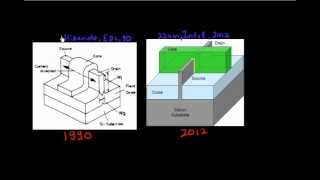
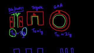
GAAFET, or Gate-All-Around FET, is a type of transistor that offers excellent electrostatic control. This means that it effectively manages how electrical charges move within the device. This enhanced control is essential for transistors operating at extremely small sizes, particularly those below 3 nanometers. As transistors shrink, controlling the flow of electrons becomes more challenging due to quantum effects, and GAAFETs address this issue by having gate material wrap around the channel from all sides.
Examples & Analogies
Think of GAAFETs like a well-designed water tank with a circular valve, where the valve controls water flow from every angle. Just as the valve effectively manages the water pressure, the GAAFET’s engineering ensures that electrical currents are controlled efficiently, resulting in better performance in smaller devices.
2D FETs - The Atomic Advantage
Chapter 2 of 5
🔒 Unlock Audio Chapter
Sign up and enroll to access the full audio experience
Chapter Content
2D FETs Atomic thickness; ideal for ultra-scaled channels
Detailed Explanation
2D FETs (Field-Effect Transistors) are distinguished by their atomic-scale thickness. This remarkable thinness enables them to effectively manage electrical channels that are extremely scaled down. Because these channels are so thin, 2D FETs can ensure that electron movement is smooth and efficient, thereby enhancing performance at lower power levels. Their structure allows for significant miniaturization while maintaining functionality.
Examples & Analogies
Imagine 2D FETs as a sheet of paper that can control traffic flow in a tiny city. The paper's thin shape means cars (electrons) can zip through efficiently, avoiding traffic jams, just as the atomic thickness allows electrons to move smoothly, enhancing the transistor’s performance.
3D ICs - A New Dimension of Integration
Chapter 3 of 5
🔒 Unlock Audio Chapter
Sign up and enroll to access the full audio experience
Chapter Content
3D ICs Integration of memory, logic, and I/O in stacked layers
Detailed Explanation
3D Integrated Circuits (ICs) represent a leap in how components like memory, logic circuits, and input/output interfaces are organized. Instead of laying flat, these components are stacked vertically, which significantly reduces space and shortens connection distances. This architecture allows for faster communication between different parts of a circuit and can lead to improved overall performance of the chip.
Examples & Analogies
Think of 3D ICs like a multi-story library. Instead of spreading all the books (components) across a single floor, stacking them saves space and allows for quicker access between different sections. Just as a library can operate more efficiently with optimized organization, 3D ICs benefit from enhanced speed and better performance.
Advanced Packaging - Optimizing Connections
Chapter 4 of 5
🔒 Unlock Audio Chapter
Sign up and enroll to access the full audio experience
Chapter Content
Advanced Packaging High-performance and low-power interconnects
Detailed Explanation
Advanced packaging techniques allow for high-performance connectivity in electronic components. This means integrating multiple chips into a single package in a way that reduces power consumption and improves signal transmission. Proper packaging is critical to reduce interference, manage heat, and ensure efficient performance, especially as components become denser and more complex.
Examples & Analogies
Consider advanced packaging like a well-organized delivery system in a busy city. Each package (chip) is connected efficiently to minimize travel time (signal transmission) and energy use (power consumption), ensuring that everything runs smoothly, just like a delivery system that prioritizes efficiency.
Neuromorphic & Quantum Devices - The Future of Computing
Chapter 5 of 5
🔒 Unlock Audio Chapter
Sign up and enroll to access the full audio experience
Chapter Content
Neuromorphic & Quantum Long-term alternatives for specific computing needs
Detailed Explanation
Neuromorphic and quantum devices represent cutting-edge approaches to computing that diverge from traditional transistor technologies. Neuromorphic devices mimic the human brain's neural architecture to process information more like humans do, which can lead to enhanced capabilities in tasks like pattern recognition. Quantum devices, leveraging principles of quantum mechanics, can tackle complex problems beyond the reach of classical computers. These technologies are seen as long-term solutions to meet evolving computational challenges.
Examples & Analogies
Imagine a neuromorphic device as a super-smart assistant who learns from every interaction, adapting to help you better with each task, similar to how our brains function. Meanwhile, quantum devices can be likened to a master chess player who can calculate numerous possibilities simultaneously, allowing it to make moves that seem impossible for regular players, addressing specific, complex computing challenges efficiently.
Key Concepts
-
GAAFET: Offers superior gate control at scales below 3nm.
-
2D FETs: Utilize atomically thick materials for enhancements in transistor characteristics.
-
3D ICs: Facilitate improved performance through vertical integration.
-
Advanced Packaging: Provides high-performance connections between stacked layers.
-
Neuromorphic Devices: Mimic neural processing, targeting AI applications.
-
Quantum Devices: Utilize principles of quantum mechanics for advanced computations.
Examples & Applications
GAAFETs are currently a focal point of research as it offers better electrostatic control, allowing for sub-3nm technology advancements.
2D material FETs illustrate the potential for ultra-scaled applications, enabling more efficient electronic designs.
Memory Aids
Interactive tools to help you remember key concepts
Rhymes
GAAFET for better gating, keeps our devices updating!
Stories
Once upon a time, in a world of electronics, GAAFETs became heroes with their superior control, helping processors scale down below the mythical size of 3nm, while 2D FETs danced across the stage showcasing their ultrathin bodies.
Memory Tools
Remember 'G2D3' - GAAFET, 2D FET, and 3D ICs for our top three technologies of the future!
Acronyms
Remember 'A.C.E' for 'Atomic, Control, Efficiency' - the goals of future technologies!
Flash Cards
Glossary
- GAAFET
Gate-All-Around Field Effect Transistor, offering superior gate control at sub-3nm nodes.
- 2D FET
Field Effect Transistor made from materials that are only a few atoms thick, allowing ultra-scaled channels.
- 3D ICs
Three-dimensional integrated circuits integrating multiple functionalities in stacked layers.
- Advanced Packaging
Techniques that enhance the interconnects between integrated circuits to improve performance.
- Neuromorphic Devices
Computing devices designed to mimic neural networks for processing data like the human brain.
- Quantum Devices
Devices that leverage quantum mechanics to perform computations that traditional devices cannot efficiently handle.
Reference links
Supplementary resources to enhance your learning experience.