
Limitations of FinFET Scaling
Interactive Audio Lesson
Listen to a student-teacher conversation explaining the topic in a relatable way.
Quantized Channel Width
🔒 Unlock Audio Lesson
Sign up and enroll to listen to this audio lesson

Today, we're going to start by discussing the quantized channel width in FinFETs. This limit affects design flexibility. Can anyone tell me what they think this might mean?

Does it mean that designers can't choose any width they want?
Exactly, it means that FinFETs have fixed width options. This limits how designers can optimize performance. Remember the acronym 'QW' for Quantized Width. Why do you think limited width could affect performance?

If the widths are fixed, it might not fit the specific requirements for every application.
Right! Customization is vital for optimizing performance in specific applications. This leads us to consider the variability in manufacturing.
Process Complexity and Cost
🔒 Unlock Audio Lesson
Sign up and enroll to listen to this audio lesson

Next, let's discuss another limitation: process complexity and cost. Why is the fabrication of FinFETs considered complex?

Because they require precise three-dimensional control?
Correct! This precision makes the fabrication more expensive and resource-intensive. Can someone share how this might impact the overall production of chips?

It could increase the price of chips, making them less accessible for consumers.
Exactly! The complex processes may drive up costs, potentially affecting market availability. Let's move on to performance variability.
Variability and Mismatch
🔒 Unlock Audio Lesson
Sign up and enroll to listen to this audio lesson
Now, please think about the concept of variability. How do you think minor differences in fin dimensions could influence FinFET performance?
Maybe it could lead to inconsistent performance outputs?
Great point! Variability leads to mismatches in performance in devices, making it tough to predict their behavior. This is crucial for yield, or the number of functional chips produced versus what's manufactured. Can anyone connect this to what we just learned about cost?
If we have more mismatches, we could end up with fewer working chips, increasing production waste and costs.
Exactly! More variability can lead to higher costs while reducing efficiency. Let's discuss electrostatic limits next.
Electrostatic Limits
🔒 Unlock Audio Lesson
Sign up and enroll to listen to this audio lesson
Electrostatic limits arise when scaling down a FinFET. Can anyone explain what happens to electrostatic control as these devices get smaller?
It gets harder for the device to control short-channel effects, right?
Yes! As we scale down, the ability to suppress these effects deteriorates, which can lead to performance degradation. Remember the acronym 'ESC' for Electrostatic Control. Moving on, what about parasitic effects?
Parasitic Capacitance and Resistance
🔒 Unlock Audio Lesson
Sign up and enroll to listen to this audio lesson
Finally, let's discuss parasitic capacitance and resistance. Why are these notable issues in dense designs?
I guess because there are more connections, increasing the unwanted effects?
Exactly! The closer components are to one another, the more these parasitic effects can influence performance negatively. This makes it difficult to maintain speed and efficiency. Can anyone summarize what we learned today?
We explored limitations like quantized widths, cost, variability, electrostatic issues, and parasitics, all of which can impact FinFET scaling!
Great recap! Understanding these challenges is vital as we look to future semiconductor technologies.
Introduction & Overview
Read summaries of the section's main ideas at different levels of detail.
Quick Overview
Standard
The section discusses various challenges encountered by FinFET technology as it approaches its scaling limits. Key issues include quantized channel widths, complexity in the fabrication process, performance variability, electrostatic limits, and significant parasitic effects due to denser designs.
Detailed
Limitations of FinFET Scaling
FinFET technology has been pivotal in advancing transistor performance in contemporary semiconductor devices, particularly as we scale down to nodes below 22nm. However, as we push the boundaries of FinFET scaling, several significant limitations arise that may hinder progression. This section delineates these limitations as follows:
- Quantized Channel Width: The design flexibility of FinFETs is constrained by the discrete options available for channel width due to their three-dimensional structure, which affects performance.
- Process Complexity and Cost: Fabricating FinFETs necessitates sophisticated 3D control and state-of-the-art lithography techniques, increasing complexity and manufacturing costs.
- Variability and Mismatch: Small variations in fin dimensions can dramatically impact performance and yield, highlighting the sensitivity of FinFET technology to manufacturing precision.
- Electrostatic Limits: As the device dimensions shrink, electrostatic control diminishes, making it increasingly difficult for FinFETs to suppress short-channel effects, which can degrade device performance.
- Parasitic Capacitance and Resistance: In densely packed configurations, parasitic capacitance and resistance become prominent, adversely affecting speed and power performance.
Overall, these limitations are critical to understanding the future trajectory of semiconductor technologies as we explore alternatives beyond FinFETs.
Youtube Videos


Audio Book
Dive deep into the subject with an immersive audiobook experience.
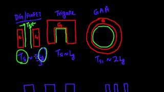
Quantized Channel Width
Chapter 1 of 5
🔒 Unlock Audio Chapter
Sign up and enroll to access the full audio experience
Chapter Content
❌ Quantized Channel Width
● FinFETs offer discrete width options, limiting design flexibility.
Detailed Explanation
FinFETs have a unique structure where the width of the channel can only take on specific, discrete values rather than being continuously adjustable. This is referred to as 'quantized channel width.' As a result, designers find it difficult to customize the channel width to meet particular performance criteria. This limitation can restrict the maximum performance capabilities that can be achieved for certain applications.
Examples & Analogies
Imagine trying to bake a cake where you can only choose certain fixed pan sizes (like 8-inch or 9-inch), rather than being able to use any size you want. This restriction in pan size means you can't create the specific cake design you envision for a given occasion.
Process Complexity and Cost
Chapter 2 of 5
🔒 Unlock Audio Chapter
Sign up and enroll to access the full audio experience
Chapter Content
❌ Process Complexity and Cost
● FinFET fabrication requires precise 3D control and advanced lithography.
Detailed Explanation
The manufacturing process of FinFETs is much more complex than that of traditional planar transistors. This complexity arises because FinFETs require precise three-dimensional control during their fabrication. Additionally, advanced lithography techniques—tools that make precise patterns on silicon wafers—must be employed, raising the overall production costs significantly. These complexities can hinder scaling and limit the economics of FinFET technology.
Examples & Analogies
Think of making a detailed sculpture out of marble. It requires specialized tools and techniques to shape the marble accurately, which can be time-consuming and expensive. If you were to compare it to molding something simpler like clay, the marble process has unique challenges that come with higher costs.
Variability and Mismatch
Chapter 3 of 5
🔒 Unlock Audio Chapter
Sign up and enroll to access the full audio experience
Chapter Content
❌ Variability and Mismatch
● Small changes in fin dimensions affect performance and yield.
Detailed Explanation
FinFETs are highly sensitive to minute variations in their structural dimensions. Even small discrepancies in the width or height of the fins can lead to significant changes in the electrical performance of the devices, as well as variations in manufacturing yields. This means that achieving consistency and reliability in performance is challenging, which can lead to increased costs and reduced efficacy in production.
Examples & Analogies
Imagine a group of people assembling bicycles. If one person slightly adjusts the length of the wheels, that bike may not ride properly compared to the others, causing inconsistency in performance. Similarly, in FinFET manufacturing, slight adjustments in design can lead to very different outcomes in how the devices operate.
Electrostatic Limits
Chapter 4 of 5
🔒 Unlock Audio Chapter
Sign up and enroll to access the full audio experience
Chapter Content
❌ Electrostatic Limits
● Beyond a certain point, FinFETs cannot suppress short-channel effects effectively.
Detailed Explanation
As FinFETs continue to scale down in size, they encounter electrostatic limitations related to short-channel effects. Specifically, as the channel length decreases, the ability of the transistor to control the current flowing through it becomes diminished. This leads to difficulties in maintaining performance as the devices become smaller, ultimately imposing a limit on how much further FinFETs can be effectively scaled.
Examples & Analogies
Think of a teacher trying to control a large classroom of students. If you make the classroom smaller and the number of students stays the same, the teacher finds it increasingly difficult to manage them effectively. Similarly, as FinFETs shrink in size, the ability to manage the flow of electricity declines, which can lead to less effective performance.
Parasitic Capacitance and Resistance
Chapter 5 of 5
🔒 Unlock Audio Chapter
Sign up and enroll to access the full audio experience
Chapter Content
❌ Parasitic Capacitance and Resistance
● Interconnect and fringe capacitance become significant in dense designs.
Detailed Explanation
In very dense designs, the effects of parasitic capacitance and resistance start to become prominent. Parasitic elements are undesired effects that occur due to the proximity of electrical components to each other, which can slow down signal transmission and increase power consumption. As more and more FinFETs are packed into a smaller area, these effects can significantly hinder the performance of the semiconductor devices, leading to inefficiencies.
Examples & Analogies
Consider a busy highway with many cars packed closely together. The closer the cars are, the more likely they are to cause traffic jams. Just like those traffic jams slow down vehicle flow, parasitic capacitance and resistance slow down electrical signals in integrated circuits, which can impact overall performance.
Key Concepts
-
Quantized Channel Width: Fixed width options limit design flexibility.
-
Process Complexity: Increased sophistication and costs in FinFET manufacturing.
-
Variability: Small dimension changes can impact performance.
-
Electrostatic Control: Diminished ability to suppress short-channel effects as size reduces.
-
Parasitic Capacitance and Resistance: Increased significance in densely packed designs.
Examples & Applications
A device designed with a channel width of 10nm may only allow for certain discrete widths such as 5nm, 7nm, or 9nm, limiting versatility.
In a production line, if 20% of manufactured chips fail due to dimensional variability, the costs escalate due to increased waste and lower yield.
Memory Aids
Interactive tools to help you remember key concepts
Rhymes
If width is fixed and not quite right, performance might not take flight.
Stories
Imagine a factory producing toys, where some workers cut pieces too big or too small. This results in mismatches, just like variabilities impacting FinFETs.
Memory Tools
Remember 'PEVQ' - Process, Electrostatic, Variability, Quantized widths to recall limitations.
Acronyms
Use 'CRES' to remember
Cost
Resistance
Electrostatic limits
Scaling issues key points.
Flash Cards
Glossary
- Quantized Channel Width
The fixed and discrete options available for the width of the channel in FinFETs, affecting design flexibility.
- Process Complexity
Refers to the sophisticated techniques required for FinFET fabrication, increasing manufacturing costs.
- Variability
The sensitivity of FinFET performance to small changes in dimensions, leading to potential mismatches.
- Electrostatic Control
The capacity of a FinFET to suppress short-channel effects, which diminishes as the device scales down.
- Parasitic Effects
Unwanted capacitance and resistance encountered within densely packed integrated circuits that affect performance.
Reference links
Supplementary resources to enhance your learning experience.