
FinFET Scaling and Future Trends
Interactive Audio Lesson
Listen to a student-teacher conversation explaining the topic in a relatable way.
Introduction to FinFET Technology
🔒 Unlock Audio Lesson
Sign up and enroll to listen to this audio lesson

Today we'll start by discussing how FinFET technology helps us continue Moore’s Law. Who can tell me what Moore’s Law entails?

Isn't it the idea that the number of transistors in a dense integrated circuit doubles about every two years?
Exactly! FinFETs have allowed us to scale down to sub-22nm nodes. Can anyone share why this scaling is important?

Because it helps us create more powerful and efficient chips that can handle more tasks.
Great point! This performance boost directly affects everything from smartphones to servers. Remember, 'More is Law!'—that's an easy way to remember why scaling is vital.
Limitations of FinFETs
🔒 Unlock Audio Lesson
Sign up and enroll to listen to this audio lesson

Now let’s dive into some limitations of FinFETs. What do you all think might be a challenge in scaling these devices further?

I think the complexity of the process might be one, right?
Yes! Process complexity is a real issue. Additionally, there's the quantized channel width. Can someone explain what that means?

It means that the width options for the FinFETs are not continuous, which limits design options!
Exactly! Keep in mind the acronym QCE—Quantized Channel Width, Complexity, and Electrostatic effects. It's a way to recall the main limitations.
Exploring Future Semiconductor Devices
🔒 Unlock Audio Lesson
Sign up and enroll to listen to this audio lesson
Let’s move on to what comes next after FinFETs. Who can name one future technology?
GAAFETs! They are better for control, right?
Absolutely! GAAFETs offer superior gate control. Who can tell me why gate control is important?
Better control leads to improved performance and reduced power consumption.
Well said! Remember the acronym 'GCC': Gate control for higher performance, Cost-effectiveness, and reduced power. This is vital for future semiconductor success.
Design and Technology Co-Optimization (DTCO)
🔒 Unlock Audio Lesson
Sign up and enroll to listen to this audio lesson
Next, let’s discuss DTCO—what do you think that implies in the context of semiconductor scaling?
I assume it means integrating engineering design with the latest technology trends?
Exactly! DTCO helps in optimizing both design and technology together. Did anyone grasp how this impacts the industry?
It could lead to more complex and efficient chips being developed more quickly!
Great insight! Think of the acronym 'DTP': Design, Technology, and Performance. This is key for driving innovation!
3D Integration and Packaging Trends
🔒 Unlock Audio Lesson
Sign up and enroll to listen to this audio lesson
Finally, let’s explore 3D integration. What are some advantages this technology brings?
It allows for stacking chips, which can save space and increase efficiency!
Absolutely right! It can also utilize formats like chiplets. Why do you think chiplets are beneficial?
Because they allow for modular designs and better customization of chips!
Fantastic observations! Remember 'SSCE': Space-saving, Scalability, Customization, and Efficiency, which summarizes the advantages of 3D integration.
Introduction & Overview
Read summaries of the section's main ideas at different levels of detail.
Quick Overview
Standard
FinFET technology has played a crucial role in the continuation of Moore’s Law at sub-22nm nodes, though it faces significant challenges as it reaches scaling limits. This section details the current trends, limitations, and potential future semiconductor devices that could replace FinFETs to ensure sustained performance improvements in the industry.
Detailed
FinFET Scaling and Future Trends
FinFET technology has facilitated continuing advancements in semiconductor devices by enabling the scaling of transistors below 22nm, supporting Moore’s Law. However, as FinFETs near their scaling limits, several key challenges arise, including channel width quantization, variability, and electrostatic limitations.
Scaling Trends in FinFET Technology
FinFETs have been adopted broadly over various technology nodes:
- 22nm: First mass usage by Intel and GlobalFoundries.
- 14nm/16nm: Mainstream adoption by TSMC, Intel, and Samsung.
- 10nm/ 7nm: High-volume production seen by TSMC, Samsung, and Intel.
- 5nm/ 3nm: Peak FinFET performance observed.
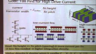
The key goals for scaling include reducing fin pitch, shortening gate lengths, lower power supply voltage, enhancing gate control, and increasing drive current.
Limitations of FinFET Scaling
Despite their advantages, FinFETs encounter bottlenecks, such as:
- Quantized Channel Width: Limits design flexibility.
- Process Complexity: Requires precise fabrication, increasing costs.
- Variability: Small fin dimension changes affect yield and performance.
- Electrostatic Limits: Ineffective short-channel effects at extreme scales.
- Parasitic Capacitance: Increases in density create significant capacitance and resistance issues.
Future Semiconductor Devices
To address these challenges, the industry explores devices beyond FinFETs:
1. GAAFETs: Provide better control with completely surrounded gates.
2. Nanosheet/Nanoribbon FETs: Higher drive currents and stackable designs.
3. V-FETs: Allow vertical current flow, ideal for 3D integration.
4. TFETs: Enable ultra-low power operation.
5. CNTFETs: Leverage carbon nanotubes for high mobility.
6. 2D Material FETs: Utilize ultra-thin body materials for better control.
Design and Technology Co-Optimization (DTCO)
Efforts to scale further focus on DTCO, combining technology advancements with design innovation and EDA tool enhancements.
3D Integration and Packaging Trends
As traditional scaling becomes impractical, alternatives such as chiplets, TSVs, and advanced packaging techniques become relevant.
Summary of Future Trends
Key future technologies include GAAFETs for better control, 2D materials for highly integrated designs, and 3D ICs for efficient performance and power integration, signaling the next wave of advancements in semiconductor technology.
Youtube Videos

Audio Book
Dive deep into the subject with an immersive audiobook experience.
Introduction to FinFET Technology
Chapter 1 of 8
🔒 Unlock Audio Chapter
Sign up and enroll to access the full audio experience
Chapter Content
FinFET technology has enabled the continuation of Moore’s Law in sub-22nm nodes by overcoming the limitations of traditional planar MOSFETs. However, as FinFETs approach their own scaling limits, new challenges and opportunities arise. This chapter explores the scaling trends, limitations, and future developments in advanced semiconductor devices beyond FinFETs.
Detailed Explanation
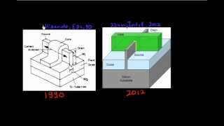
FinFET technology has been crucial for continuing Moore's Law at very small manufacturing sizes, specifically below 22 nanometers. This means that the number of transistors that can fit on a computer chip continues to double approximately every two years, increasing performance and reducing cost per transistor. Despite its advantages, FinFETs are starting to reach their physical limits in terms of size and performance, which leads to both challenges—like increased complexity—and opportunities for innovation. The chapter discusses not only the past successes of FinFETs but also what lies ahead in terms of new technologies.
Examples & Analogies
Think of FinFETs like skyscrapers in a city. Just as builders have found ways to add floors to make the most of a small plot of land, FinFETs allow us to add more transistors to small chip sizes. However, like a city that can only build so tall before it runs into zoning laws and structural limits, FinFET technology is reaching its upper limits.
Scaling Trends in FinFET Technology
Chapter 2 of 8
🔒 Unlock Audio Chapter
Sign up and enroll to access the full audio experience
Chapter Content
FinFETs have been widely adopted in advanced nodes:
Technology Foundry Examples FinFET Adoption
Node
22nm Intel, GlobalFoundries First mass FinFET usage
14nm/16nm Intel, TSMC, Samsung Mainstream adoption
10nm / 7nm TSMC, Samsung, Intel High-volume production
5nm / 3nm TSMC, Samsung Peak FinFET performance
Key Scaling Goals:
● Smaller Fin Pitch (distance between fins)
● Shorter Gate Lengths (Lg)
● Lower VDD for power reduction
● Better gate control using multi-gate structures
● Higher drive current with taller fins
Detailed Explanation
The adoption of FinFET technology has occurred progressively across various technology nodes, starting from 22nm down to 3nm. Each node represents a level of advancement in manufacturing sizes and transistor density, with key foundries like Intel and TSMC at the forefront. The chapter points out crucial scaling goals for optimizing FinFET technology, which include reducing the distance between fins (fin pitch), shortening the gate lengths, and lowering voltage for power savings while improving control of the gate structure.
Examples & Analogies
Imagine building a more efficient transportation network. Just as planners aim to have roads closer together and shorter distances to travel, engineers work to optimize the placement of transistor components on chips to achieve better performance. Each new node in semiconductor technology represents an improved 'road network' that allows for better 'traffic flow' in terms of data processing.
Limitations of FinFET Scaling
Chapter 3 of 8
🔒 Unlock Audio Chapter
Sign up and enroll to access the full audio experience
Chapter Content
Despite their advantages, FinFETs face several bottlenecks as they scale:
❌ Quantized Channel Width
● FinFETs offer discrete width options, limiting design flexibility.
❌ Process Complexity and Cost
● FinFET fabrication requires precise 3D control and advanced lithography.
❌ Variability and Mismatch
● Small changes in fin dimensions affect performance and yield.
❌ Electrostatic Limits
● Beyond a certain point, FinFETs cannot suppress short-channel effects effectively.
❌ Parasitic Capacitance and Resistance
● Interconnect and fringe capacitance become significant in dense designs.
Detailed Explanation
As effective as FinFET technology has been, it encounters several limitations as engineers attempt to scale it down further. For instance, the width of the channel in FinFETs is 'quantized,' meaning that design options are limited to specific sizes. Additionally, manufacturing FinFETs is complex and costly due to the advanced techniques required. Changes in dimensions can also lead to performance inconsistencies, making yields unpredictable. Moreover, as device sizes shrink, electrostatic control deteriorates, and unwanted capacitance and resistance start affecting overall performance.
Examples & Analogies
Consider cooking in a very small kitchen. While you can optimize space by using specialized utensils (like the fins in FinFET designs), there are only so many tools you can fit in the cabinets (the limits of design flexibility). You also need precise measurements and techniques to ensure everything cooks properly, but if the stove's performance drops due to overcrowding, your meal—like the transistor's performance—could suffer.
Beyond FinFET: Future Semiconductor Devices
Chapter 4 of 8
🔒 Unlock Audio Chapter
Sign up and enroll to access the full audio experience
Chapter Content
As FinFETs approach physical limits, the semiconductor industry is exploring post-FinFET devices to sustain performance improvements:
-
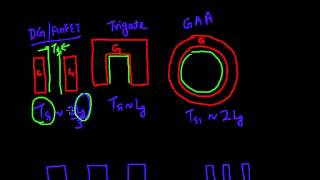
Gate-All-Around FETs (GAAFETs)
● Replaces the fin with nanowires or nanosheets completely surrounded by the gate.
● Offers superior gate control compared to FinFETs. -
Nanosheet/Nanoribbon FETs
● Wider channels than nanowires → higher drive current.
● Stackable design improves density. -
Vertical FETs (V-FETs)
● Current flows vertically from source to drain.
● Promising for 3D IC integration. -
Tunneling FETs (TFETs)
● Operate using band-to-band tunneling instead of thermionic emission.
● Potential for sub-60 mV/dec subthreshold slope (ideal for ultra-low power). -
Carbon Nanotube FETs (CNTFETs)
● Use of carbon nanotubes for the channel.
● High mobility and potential for ballistic transport. -
2D Material FETs
● Channels made from materials like MoS₂, WS₂, graphene.
● Ultra-thin body offers excellent gate control.
Detailed Explanation
With the limitations of FinFETs in mind, researchers are looking into various new technologies that can continue to enhance performance. These include: GAAFETs, which improve gate control; nanosheet FETs that allow higher current; vertical FETs for 3D configurations; TFETs that promise lower power usage; CNTFETs utilizing the properties of carbon nanotubes; and 2D material FETs employing ultra-thin materials for superior control. This exploration is essential for sustaining advancements in semiconductor technology.
Examples & Analogies
Envision a smartphone company constantly refining its design to improve battery life and performance. Just like they might switch from a conventional battery to a more advanced one, the semiconductor industry is switching from FinFETs to more innovative materials and designs to achieve better efficiency and effectiveness.
Design and Technology Co-Optimization (DTCO)
Chapter 5 of 8
🔒 Unlock Audio Chapter
Sign up and enroll to access the full audio experience
Chapter Content
To scale further, the industry is focusing on DTCO, which integrates:
● Technology scaling (materials, dimensions)
● Design innovations (new standard cell libraries, quantized fin-aware logic)
● EDA tool enhancement for layout, modeling, and verification
Detailed Explanation
Design and Technology Co-Optimization (DTCO) is a method the semiconductor industry uses to promote efficiency and performance. This strategy involves aligning technological advancements—like materials and dimensions—with innovative design practices, such as the creation of new electronic components and tools for electronic design automation (EDA). Ultimately, DTCO ensures that as one element evolves, so does the other, maximizing chip performance and scalability.
Examples & Analogies
Think of DTCO like a car designer who collaborates closely with engineers. As the design for a new car body is developed, the engineering team simultaneously refines the engine and other components to ensure everything works harmoniously, resulting in a high-performing vehicle. In semiconductors, if the design changes, the manufacturing process must adapt to keep up with those innovations.
3D Integration and Packaging Trends
Chapter 6 of 8
🔒 Unlock Audio Chapter
Sign up and enroll to access the full audio experience
Chapter Content
As planar scaling becomes cost-prohibitive, 3D ICs and heterogeneous integration offer alternatives:
● Chiplets: Modular components integrated on a shared package (e.g., AMD’s Ryzen CPUs)
● TSVs (Through-Silicon Vias): For vertical stacking of dies
● Advanced packaging (e.g., Intel Foveros, TSMC CoWoS, Samsung X-Cube)
Detailed Explanation
With the challenges of maintaining performance through conventional scaling, manufacturers are now exploring 3D integration and packaging techniques. Chiplets are smaller, modular pieces that can be combined in a shared package, making them flexible and efficient. Through-Silicon Vias (TSVs) allow for vertical stacking of chip components, further enhancing integration. Advanced packaging methods also play a critical role in improving performance while reducing space and cost.
Examples & Analogies
Imagine a multi-story building with modular apartments where each floor represents a chiplet. The building design allows families to live together but occupy less land than building multiple homes separately. Similarly, 3D integration uses vertical space to enhance semiconductor functionality without expanding its footprint too wide, just as the building makes efficient use of height.
Summary of Future Trends
Chapter 7 of 8
🔒 Unlock Audio Chapter
Sign up and enroll to access the full audio experience
Chapter Content
Technology Key Benefit
GAAFETs Best electrostatic control for sub-3nm nodes
2D FETs Atomic thickness; ideal for ultra-scaled channels
3D ICs Integration of memory, logic, and I/O in stacked layers
Advanced Packaging High-performance and low-power interconnects
Neuromorphic & Quantum Long-term alternatives for specific computing needs Devices
Detailed Explanation
The chapter concludes with a summary of promising technologies that could shape the future of semiconductors. GAAFETs will likely succeed FinFETs in sub-3nm applications. 2D FETs, with their minimal thickness, will allow for further scaling. 3D ICs will integrate various functions in one package, making them efficient. Advanced packaging will support faster connections while saving power. Neuromorphic and quantum devices represent potential future alternatives aimed at specific computing demands.
Examples & Analogies
It’s like a toolkit that evolves over time. As new projects and challenges arise, we can’t just keep using the same old tools. Instead, we develop new tools (like GAAFETs and 3D ICs) that are better suited for the upcoming tasks. Just as a modern toolkit may include a high-tech laser cutter and 3D printer, the semiconductor industry must innovate to meet future processing needs.
Summary of Key Concepts
Chapter 8 of 8
🔒 Unlock Audio Chapter
Sign up and enroll to access the full audio experience
Chapter Content
● FinFETs have supported Moore’s Law from 22nm down to 3nm, but now face physical and economic limits.
● Next-generation devices like GAAFETs, nanosheets, and 2D FETs promise continued scaling.
● The future of electronics involves a combination of new device architectures, 3D integration, and co-optimization between design and technology.
Detailed Explanation
This summary highlights the journey of FinFETs in enabling rapid advancements in technology but also indicates the pressing need for innovation beyond FinFETs due to emerging limitations. Notable upcoming devices such as GAAFETs and 2D FETs signify a shift towards maintaining progress and overcoming these challenges. Furthermore, the growth of electronics will increasingly depend on integrating new device structures, vertical designs, and harmony between design and manufacturing processes.
Examples & Analogies
Think of the evolution of mobile phones. As capabilities expanded, some technologies from earlier models became obsolete, while new designs emerged to meet users’ demands. Similarly, as transistors have approached their limits, the semiconductor industry must adapt and innovate to create smarter and more efficient chips, just like how mobile technology has progressed to meet modern needs.
Key Concepts
-
FinFET Technology: A pivotal innovation for scaling down transistors.
-
Limitations of FinFET: Challenges such as quantized channel widths and process complexity.
-
Future Technologies: New devices like GAAFETs and 3D ICs promise to continue performance improvements.
-
Design and Technology Co-Optimization (DTCO): Integrating design with technological advancement.
-
3D Integration: Offers space efficiency and enhanced performance through stacking technologies.
Examples & Applications
FinFETs are widely used in many modern processors, such as those found in data centers and mobile devices.
GAAFETs are being researched to replace traditional FinFETs in sub-3nm technology nodes, promising enhanced electrostatic control.
Memory Aids
Interactive tools to help you remember key concepts
Rhymes
For faster chips and less heat, FinFET's the scaling feat!
Stories
Once upon a time, chips were flat and just did their bit. But then came the FinFETs, tall and finned, they took performance on a win!
Memory Tools
Remember GAAFET: Great At Advanced Field effects, enhancing control!
Acronyms
DTCO
Design Tech Co-Optimize for the perfect performance!
Flash Cards
Glossary
- FinFET
A type of non-planar transistor used in advanced semiconductor devices to improve control over the channel.
- Moore’s Law
The observation that the number of transistors on a microchip doubles approximately every two years, leading to an increase in performance.
- GAAFET
Gate-All-Around Field Effect Transistor, a transistor design providing better electrostatic control through a gate that surrounds the conducting channel.
- Nanosheet
A type of transistor design utilizing nanosheets for increased drive current and improved density.
- 3D IC
Three-dimensional integrated circuit, which involves stacking multiple layers of circuits to enhance performance and reduce area.
- DTCO
Design and Technology Co-Optimization, a strategy that integrates design considerations with technology advancement to optimize semiconductor performance.
Reference links
Supplementary resources to enhance your learning experience.