
Summary of Key Concepts
Interactive Audio Lesson
Listen to a student-teacher conversation explaining the topic in a relatable way.
Introduction to FinFET Technology
🔒 Unlock Audio Lesson
Sign up and enroll to listen to this audio lesson

Welcome, class! Today, we will explore FinFET technology and its impact on Moore's Law. Can anyone tell me what FinFET stands for?

FinFET stands for Fin Field Effect Transistor, right?
Correct! FinFETs have allowed us to scale down to 3nm. Can anyone think of why scaling down is necessary?

It's important for increasing performance and reducing power consumption!
Exactly! But as we scale down, we face limits. Can anyone name a limit we might encounter?

Isn't there something called electrostatic limits?
Yes! That's one of the key limitations we face today.
In summary, we see that while FinFETs have supported Moore's Law, new challenges are emerging as we approach 3nm and beyond.
Emerging Technologies
🔒 Unlock Audio Lesson
Sign up and enroll to listen to this audio lesson

Now let's discuss what comes after FinFETs. What do you think are some potential next-generation technologies?

I think GAAFETs are one of them!
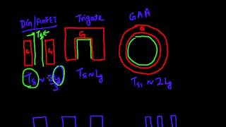
That's right! GAAFETs offer better electrostatic control. Can anyone tell me how GAAFETs differ from FinFETs?
GAAFETs use nanowires that are completely surrounded by the gate!
Correct! This allows for superior control compared to the fins in FinFETs. What about nanosheets?
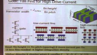
Nanosheets have wider channels, which could lead to higher drive currents!
Excellent! Wide channels do improve current. So, in summary, GAAFETs and nanosheets are promising new architectures that may help in the future.
Integration Techniques
🔒 Unlock Audio Lesson
Sign up and enroll to listen to this audio lesson
In addition to new device architectures, integration is becoming crucial. What are some examples of integration techniques?
3D integration using chiplets!
Yes! And why is 3D integration advantageous?
It allows for stacking components to save space and improve performance!
Exactly! Additionally, Design Technology Co-Optimization, or DTCO, helps to enhance device performance through synergistic design and technology improvements.
To summarize, the integration of new device architectures and techniques like 3D integration is essential for the future of electronics.
Introduction & Overview
Read summaries of the section's main ideas at different levels of detail.
Quick Overview
Standard
As FinFET technology meets physical and economic limits, this section reviews its role in supporting Moore’s Law and highlights emerging technologies such as GAAFETs, nanosheets, and 2D materials that could enable continued scaling in semiconductor devices. The future landscape of electronics is seen as increasingly reliant on new device architectures and integration techniques.
Detailed
Summary of Key Concepts
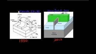
- FinFET Technology: FinFETs have been crucial in continuation of Moore’s Law in nodes from 22nm to 3nm. However, as we approach these limits, both physical and economic challenges arise.
- Next-Generation Devices: Emerging technologies, including Gate-All-Around FETs (GAAFETs), nanosheets, and 2D FETs, offer potential methods for sustaining scaling. These devices promise superior performance and efficiency compared to traditional FinFETs.
- Integration Techniques: The evolution of semiconductor technology also emphasizes the importance of 3D integration and design-technology co-optimization to further enhance performance and reduce sizes.
Youtube Videos

Audio Book
Dive deep into the subject with an immersive audiobook experience.
FinFETs and Moore's Law
Chapter 1 of 3
🔒 Unlock Audio Chapter
Sign up and enroll to access the full audio experience
Chapter Content
● FinFETs have supported Moore’s Law from 22nm down to 3nm, but now face physical and economic limits.
Detailed Explanation
This statement highlights the significant role that FinFET technology has played in advancing semiconductor device scaling under Moore's Law, which predicts that the number of transistors on a chip will double approximately every two years, leading to increased performance and reduced costs. FinFETs allowed this trend to continue as technology shrank from 22nm (nanometers) down to 3nm. However, the technology is now encountering both physical challenges (like quantum effects and power loss) and economic barriers (such as high production costs), which limit further scaling.
Examples & Analogies
Think of FinFETs like a series of row houses that could be built closer together. As you keep adding more houses (transistors) on a street, you can fit in many more until you run out of space and face issues like building regulations (physical limits) or rising construction costs (economic limits).
Future Device Architectures
Chapter 2 of 3
🔒 Unlock Audio Chapter
Sign up and enroll to access the full audio experience
Chapter Content
● Next-generation devices like GAAFETs, nanosheets, and 2D FETs promise continued scaling.
Detailed Explanation
This point introduces exciting future technologies that could replace or enhance FinFETs, thus continuing the trend of miniaturization and performance enhancement in semiconductor devices. GAAFETs (Gate-All-Around FETs) improve gate control by wrapping it fully around the channel, while nanosheets and 2D FETs use materials that are thinner and potentially more efficient. These innovations aim to push the boundaries of how small and efficient chips can become, addressing the issues that FinFETs will increasingly face as they reach their limits.
Examples & Analogies
Imagine upgrading from a traditional light bulb to an LED bulb. The LED bulb is much smaller and more efficient (like nanosheets and 2D FETs) while providing the same or greater amount of light. GAAFETs are like a new smart bulb that can adjust its brightness and color based on the room's needs, thus offering better control and efficiency.
The Future of Electronics
Chapter 3 of 3
🔒 Unlock Audio Chapter
Sign up and enroll to access the full audio experience
Chapter Content
● The future of electronics involves a combination of new device architectures, 3D integration, and co-optimization between design and technology.
Detailed Explanation
This final point emphasizes that the evolution of electronics will not only rely on the development of new device types but also integrate different approaches such as 3D integration—stacking chips to save space and improve performance—and co-optimization, which aligns design processes with technological advancements. This means that as new devices are developed, corresponding design techniques and strategies will be refined, ensuring that each new advancement leads to better overall performance and efficiency.
Examples & Analogies
Think about a car where all parts, from the engine to the tires, need to work together for optimum performance. If you upgrade the engine but ignore the tires, the car won't perform well. Similarly, in the future of electronics, advancements in chip design and architecture must work in harmony to ensure maximum efficiency and functionality.
Key Concepts
-
FinFET Technology: A crucial advancement to continue scaling in semiconductor technology down to 3nm.
-
Next-Generation Devices: Emerging technologies like GAAFETs and nanosheets offer better performance.
-
Integration Techniques: 3D integration and DTCO are vital for future advancements in electronics.
Examples & Applications
FinFETs enable manufacturers to produce smaller and more efficient chips, thus keeping up with the pace of Moore's Law.
GAAFETs allow for better control of electrical currents, leading to potential improvements in power consumption and performance in future devices.
Memory Aids
Interactive tools to help you remember key concepts
Rhymes
FinFETs help us scale and grow, but limits now start to show.
Stories
Imagine a city where buildings can only grow so tall; the taller they grow, the more they sway. FinFETs are like those tall buildings, reaching their limits, inspiring new designs like GAAFETs and nanosheets.
Memory Tools
Remember GAAFETs and nanosheets as 'Great Advances For Easy Transactions'.
Acronyms
3D stands for 'Dynamic Design in Depth'.
Flash Cards
Glossary
- FinFET
A type of multi-gate transistor where the conducting channel is formed by a thin fin-shaped structure.
- Moore’s Law
The observation that the number of transistors on a microchip doubles approximately every two years.
- GAAFET
Gate-All-Around FET, a transistor architecture that uses a gate electrode to control the channel from all sides.
- Nanosheet
A type of transistor structure featuring flat sheets of semiconductor material to improve performance.
- 2D FET
A type of transistor that employs two-dimensional materials like graphene for the channel.
- 3D Integration
The process of stacking semiconductor components vertically to improve performance and reduce space.
- DTCO
Design-Technology Co-Optimization; a strategy that aligns design and fabrication processes for optimal performance.
Reference links
Supplementary resources to enhance your learning experience.