
Beyond FinFET: Future Semiconductor Devices
Interactive Audio Lesson
Listen to a student-teacher conversation explaining the topic in a relatable way.
Gate-All-Around FETs (GAAFETs)
🔒 Unlock Audio Lesson
Sign up and enroll to listen to this audio lesson

Today, we're going to discuss Gate-All-Around FETs, commonly known as GAAFETs. Can anyone tell me why superior gate control is significant in semiconductor devices?

It helps in reducing power loss and improving performance, right?
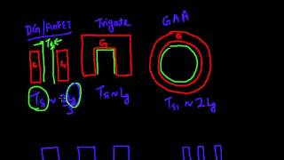
Exactly! GAAFETs encircle the channel with the gate, providing much better control over the electrostatic potential. This means that they can effectively regulate the flow of current, especially in smaller nodes like sub-3nm. Can anyone think of applications where such properties would be beneficial?

Maybe in mobile devices that need to be very energy-efficient?
Absolutely! Devices like smartphones would benefit greatly from GAAFETs. Remember, GAAFETs stand for 'Gate-All-Around FET'—that’s a handy mnemonic. Let’s summarize: GAAFETs provide better gate control than FinFETs and are essential for future technologies.
Nanosheet/Nanoribbon FETs
🔒 Unlock Audio Lesson
Sign up and enroll to listen to this audio lesson

Next, let’s delve into Nanosheet and Nanoribbon FETs. What do you think are the advantages of having wider channels?

Wider channels can support higher drive currents, right?
Correct! But that’s not all. They also offer a stackable design that increases density. Can anyone explain why density in chips is important?

Higher density means we can fit more transistors in a smaller space, improving performance!
Exactly! Higher transistor density directly correlates with better performance. A quick acronym to remember here is 'NANOs are wider!'—NANO for 'Nanosheet/Nanoribbon' and remembering their width advantage.
This helps with scaling, especially as we move toward future nodes.
Great observation! So remember, Nanosheet/Nanoribbon FETs are advantageous for higher drive currents and improved transistor density.
Vertical FETs (V-FETs)
🔒 Unlock Audio Lesson
Sign up and enroll to listen to this audio lesson
Let’s talk about Vertical FETs, or V-FETs. What’s the significance of having current flow vertically?
It allows for 3D IC integration, doesn't it?
Absolutely! 3D integration allows for more efficient use of space and power. Can anyone think of why this might be necessary in modern computing?
There’s a demand for more powerful chips that can run complex applications!
Exactly right! V-FETs are essential for meeting that demand. Keep in mind the phrase 'Vertical Vision' to remember that these devices operate with vertical current flow.
Tunneling FETs (TFETs)
🔒 Unlock Audio Lesson
Sign up and enroll to listen to this audio lesson
Moving on, let’s discuss Tunneling FETs, or TFETs. Who can explain what band-to-band tunneling is?
It’s when electrons can tunnel from one energy band to another!
Correct! This allows for a sub-60 mV/dec subthreshold slope, which is crucial for ultra-low power applications. Any thoughts on how this could impact device efficiency?
It means they can operate at much lower voltage levels, reducing energy consumption!
Exactly, that’s a critical advantage. As a memory aid, think 'TFET for Tomorrow’s Future Energy Technology'—this highlights their efficiency goals.
Introduction & Overview
Read summaries of the section's main ideas at different levels of detail.
Quick Overview
Standard
As FinFET technology approaches its physical limits, this section explores various future semiconductor devices, such as GAAFETs and nanosheet FETs, emphasizing their superior performance characteristics for next-generation applications.
Detailed
Beyond FinFET: Future Semiconductor Devices
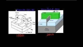
As the semiconductor industry faces the physical limits of FinFET technology, new device architectures are being explored to continue performance improvements. This section introduces several post-FinFET device types:
- Gate-All-Around FETs (GAAFETs): GAAFETs utilize nanowires or nanosheets completely surrounded by the gate, which provides better electrostatic control than FinFETs, making them suitable for sub-3nm technologies.
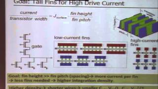
- Nanosheet/Nanoribbon FETs: These FETs have wider channels than traditional nanowires, leading to higher drive currents. Their stackable design also enhances chip density, which is critical for meeting future performance demands.
- Vertical FETs (V-FETs): In V-FETs, current flows vertically from source to drain. This configuration is promising for 3D IC integration, enabling more compact designs with improved performance.
- Tunneling FETs (TFETs): TFETs employ band-to-band tunneling rather than thermionic emission, allowing for a sub-60 mV/dec subthreshold slope, which is advantageous for ultra-low power applications.
- Carbon Nanotube FETs (CNTFETs): Utilizing carbon nanotubes as channels, CNTFETs offer high electron mobility and the potential for ballistic transport, which means reduced energy dissipation.
- 2D Material FETs: Devices made from materials like molybdenum disulfide (MoS₂), tungsten disulfide (WS₂), or graphene provide ultra-thin channel bodies, which facilitate excellent gate control and performance.
In summary, these advancements in semiconductor devices present significant opportunities for continued scaling and integration, essential for maintaining technological growth in electronic devices beyond the limitations now faced by FinFETs.
Youtube Videos

Audio Book
Dive deep into the subject with an immersive audiobook experience.
Gate-All-Around FETs (GAAFETs)
Chapter 1 of 6
🔒 Unlock Audio Chapter
Sign up and enroll to access the full audio experience
Chapter Content
- Gate-All-Around FETs (GAAFETs)
- Replaces the fin with nanowires or nanosheets completely surrounded by the gate.
- Offers superior gate control compared to FinFETs.
Detailed Explanation
GAAFETs represent an advanced transistor design that enhances gate control around the channel. Traditional FinFETs have fins that extend vertically, but GAAFETs use nanowires or nanosheets that are enclosed on all sides by the gate material. This 3D structure provides much better control over the electric field around the channel, which improves the device's performance and reduces power consumption. Essentially, having the gate surrounded on all sides prevents leakage currents and allows for better on-off switching characteristics.
Examples & Analogies
Imagine a garden surrounded by a high fence on all sides. Just as the fence provides better control over what goes in and out of the garden, the GAAFET’s surrounding gate provides better control over the electrical current flowing through the transistor.
Nanosheet/Nanoribbon FETs
Chapter 2 of 6
🔒 Unlock Audio Chapter
Sign up and enroll to access the full audio experience
Chapter Content
- Nanosheet/Nanoribbon FETs
- Wider channels than nanowires → higher drive current.
- Stackable design improves density.
Detailed Explanation
Nanosheet or nanoribbon technology uses wider channels compared to the traditional nanowire designs. This increased width allows for higher drive currents, which translates to improved performance in terms of speed and efficiency. Additionally, because these sheets can be stacked vertically, they enhance device density — meaning more transistors can fit into a smaller area, which is crucial for continuing to scale down electronic components.
Examples & Analogies
Think of nanosheets like layers of pancakes. Each pancake represents a transistor, and the wider the pan, the more pancakes (transistors) can fit in the same space. This stacking ability optimizes space and efficiency.
Vertical FETs (V-FETs)
Chapter 3 of 6
🔒 Unlock Audio Chapter
Sign up and enroll to access the full audio experience
Chapter Content
- Vertical FETs (V-FETs)
- Current flows vertically from source to drain.
- Promising for 3D IC integration.
Detailed Explanation
Vertical FETs take advantage of vertical current flow, which allows for a more compact design compared to traditional horizontal designs. This vertical structure is particularly promising for 3D integrated circuit (IC) configurations, where multiple layers of transistors can be integrated more cleanly and efficiently. This leads to faster connections between components and potentially lower power consumption overall because of the reduced distance current must travel.
Examples & Analogies
Envision a multi-story building where elevators (current) can go up and down instead of needing to travel horizontally between offices. This vertical movement allows for quicker access and more efficient use of space within the building.
Tunneling FETs (TFETs)
Chapter 4 of 6
🔒 Unlock Audio Chapter
Sign up and enroll to access the full audio experience
Chapter Content
- Tunneling FETs (TFETs)
- Operate using band-to-band tunneling instead of thermionic emission.
- Potential for sub-60 mV/dec subthreshold slope (ideal for ultra-low power).
Detailed Explanation
Tunneling FETs utilize a principle called band-to-band tunneling to allow current to flow even when the gate voltage is very low. This is fundamentally different from traditional FETs, which rely on heating and thermionic emission. The unique operation of TFETs can achieve steep subthreshold slopes (less than 60 mV/decade), making them extremely efficient for low-power applications. This efficiency is particularly valuable in mobile devices, where battery life is crucial.
Examples & Analogies
Imagine a water slide that lets you splash down even if you're barely pushing off the top. Similarly, TFETs allow current to flow with much less energy required, which could help devices use less battery power while still delivering power.
Carbon Nanotube FETs (CNTFETs)
Chapter 5 of 6
🔒 Unlock Audio Chapter
Sign up and enroll to access the full audio experience
Chapter Content
- Carbon Nanotube FETs (CNTFETs)
- Use of carbon nanotubes for the channel.
- High mobility and potential for ballistic transport.
Detailed Explanation
Carbon Nanotube FETs utilize carbon nanotubes as the channel material, which offers exceptional electrical properties. These materials allow for incredibly high charge carrier mobility, enabling faster switching speeds and potentially lower power consumption. The ability for ballistic transport — where electrons travel without scattering — means that CNTFETs can achieve performance levels significantly higher than conventional silicon-based devices.
Examples & Analogies
Think of electrons moving through carbon nanotubes like cars on a smooth highway versus a bumpy back road. On the highway, cars (electrons) can travel faster and with less effort, similar to how CNTFETs enable faster electronic devices.
2D Material FETs
Chapter 6 of 6
🔒 Unlock Audio Chapter
Sign up and enroll to access the full audio experience
Chapter Content
- 2D Material FETs
- Channels made from materials like MoS₂, WS₂, graphene.
- Ultra-thin body offers excellent gate control.
Detailed Explanation
2D Material FETs leverage materials that are only a few atoms thick, such as molybdenum disulfide (MoS₂) or graphene. The ultra-thin structure allows for outstanding control of the channel by the gate, leading to better performance characteristics and less power consumption. By using these 2D materials, engineers can build transistors with extremely small dimensions, which is critical as we continue to strive for smaller and faster electronic components.
Examples & Analogies
Consider how a very thin, flexible sheet can be easily folded into intricate shapes. Similarly, 2D materials permit intricate designs at a nanoscale, allowing for innovative electronic circuits that wouldn’t be possible with traditional materials.
Key Concepts
-
GAAFETs: Improved gate control and better electrostatic management for smaller nodes.
-
Nanosheet/Nanoribbon FETs: Wider channels and enhanced density for improved performance.
-
Vertical FETs (V-FETs): Facilitate more compact device structures through vertical current flow.
-
Tunneling FETs (TFETs): Enable low voltage operation through band-to-band tunneling.
-
Carbon Nanotube FETs (CNTFETs): High mobility channels with potential for ballistic transport.
-
2D Material FETs: Utilization of materials like MoS₂ for excellent control in ultra-thin devices.
Examples & Applications
GAAFETs are ideal for mobile devices where low power consumption and high performance are crucial.
Nanosheet FETs can be used in applications requiring dense and high-speed computing capabilities.
V-FETs aid in creating compact chip designs in cutting-edge computing technologies.
TFETs are likely candidates for next-generation low-power electronic gadgets.
Memory Aids
Interactive tools to help you remember key concepts
Rhymes
For GAAFETs, gates all around, keep control tight, performance is profound.
Stories
Imagine a futuristic lab where scientists create devices that are as small as a speck of dust, but powerful enough to control entire networks. They use nanosheets to stack and widen the spacings of currents to achieve speeds and performance previously thought impossible!
Memory Tools
For TFETs: T stands for Tunneling, F for Future efficiency and E for Energy conservation.
Acronyms
Remember GAAFETs as 'Greatly Advanced Gate-All-Around FETs'.
Flash Cards
Glossary
- GAAFET
Gate-All-Around FET, a type of transistor that has a gate that surrounds the channel on all sides to improve electrostatic control.
- Nanosheet/Nanoribbon FETs
Transistors that use nanosheets or nanoribbons as channels, offering higher drive currents and superior stacking capabilities.
- Vertical FETs (VFETs)
Transistors designed for vertical current flow, facilitating 3D integrated circuits.
- Tunneling FETs (TFETs)
Transistors that operate on the principle of band-to-band tunneling, providing low voltage operation levels.
- Carbon Nanotube FETs (CNTFETs)
Transistors that utilize carbon nanotubes for their channel, allowing high mobility and reduced energy loss.
- 2D Material FETs
Transistors made from two-dimensional materials like MoS₂, known for excellent gate control.
Reference links
Supplementary resources to enhance your learning experience.