
3D Integration and Packaging Trends
Interactive Audio Lesson
Listen to a student-teacher conversation explaining the topic in a relatable way.
Introduction to 3D ICs and the Need for Integration
🔒 Unlock Audio Lesson
Sign up and enroll to listen to this audio lesson

Today we will explore the significant shift towards 3D Integration in semiconductor design. With planar scaling becoming increasingly unaffordable, companies are examining alternatives like 3D ICs.

Why is planar scaling becoming cost-prohibitive?
Good question! As we push the limits of technology, manufacturing processes become more complex and expensive. The costs involved in producing smaller chips can far outweigh the benefits as we approach these limits.

So how do 3D ICs help with these costs?
3D ICs utilize chiplets, or modular components, which can be designed separately and integrated into a single package. This means we can optimize individual functions without redesigning everything, reducing overall expenses.

Can you give an example of where this has been successfully implemented?
Definitely! AMD’s Ryzen CPUs are a prime example of productivity through chiplets. Each chiplet can be optimized for specific tasks, enhancing overall performance and efficiency.
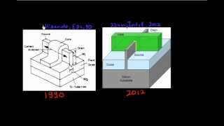
Understanding Through-Silicon Vias (TSVs)
🔒 Unlock Audio Lesson
Sign up and enroll to listen to this audio lesson

Now let’s talk about Through-Silicon Vias or TSVs. Does anyone know what they are?

Aren't they used to connect different layers of a chip?
Exactly! TSVs create vertical interconnects through silicon wafers, which allows for more compact designs and shorter signaling distances. This leads to faster data transfer rates.
Are there any drawbacks to using TSVs?
Yes, while TSVs indeed have benefits, they can also introduce complexities in manufacturing and increase costs due to the additional processing required.
What companies are leading the way with TSV technologies?
Intel, TSMC, and Samsung are notable leaders in utilizing TSV technology as part of their advanced packaging solutions to create better-integrated circuits.
Exploration of Advanced Packaging Technologies
🔒 Unlock Audio Lesson
Sign up and enroll to listen to this audio lesson
Next, let’s delve into advanced packaging technologies. Who can tell me about some examples we've discussed?
I remember we talked about Intel Foveros. What exactly does it do?
Great recall! Intel Foveros facilitates a stacked architecture, allowing active components to be placed on top of one another, optimizing space and improving performance.
What about TSMC CoWoS?
Good point! TSMC's CoWoS, or Chip on Wafer on Substrate, integrates various chips in a single package to enhance performance while managing higher bandwidth and better power efficiency.
The Future of 3D Integration
🔒 Unlock Audio Lesson
Sign up and enroll to listen to this audio lesson
Finally, let’s discuss the future impact of 3D integration and packaging. How do you think this will change chip designs?
I believe it will allow for better performance in more compact designs, which would be critical for mobile technology.
Will this kind of packaging reduce power consumption too?
You're on the right track! By reducing the distance between components and utilizing more efficient power distribution methods, we certainly expect power consumption to decrease.
Are there also challenges we should be aware of?
Indeed! While the benefits are substantial, we must watch out for thermal management issues and manufacturing complexities.
So, what’s the takeaway here?
3D integration and advanced packaging represent the future of semiconductor technology, allowing for continued growth in performance and efficiency while overcoming the limitations of traditional approaches.
Introduction & Overview
Read summaries of the section's main ideas at different levels of detail.
Quick Overview
Standard
As Moore's Law approaches its limits in terms of cost-effectiveness, the industry is shifting focus towards 3D integration and advanced packaging. Key methodologies such as chiplets, through-silicon vias (TSVs), and advanced packaging technologies like Intel's Foveros and TSMC's CoWoS are highlighted for their roles in improving device performance and integration density.
Detailed
3D Integration and Packaging Trends
As the semiconductor industry faces the economic challenges of continued planar scaling, the development of 3D Integrated Circuits (3D ICs) and heterogeneous integration has emerged as a viable alternative. Unlike traditional methods that rely heavily on 2D scaling, 3D ICs incorporate chiplet architectures, which are modular components encapsulated within a shared package. This approach allows for a more flexible and cost-efficient design process, as seen in AMD’s Ryzen CPUs.
Additionally, Through-Silicon Vias (TSVs) are discussed as a technology enabling the vertical stacking of dies, which significantly enhances the functionality and performance of integrated circuits. The section further details advanced packaging solutions like Intel’s Foveros, TSMC’s CoWoS, and Samsung’s X-Cube, which collectively illustrate the ongoing innovation within semiconductor packaging to accommodate diverse functional requirements while promoting greater efficiency and reducing power consumption. This transition reflects a significant trend beyond traditional scaling, addressing both physical and economic limitations in the semiconductor landscape.
Youtube Videos
Audio Book
Dive deep into the subject with an immersive audiobook experience.
Introduction to 3D ICs and Heterogeneous Integration
Chapter 1 of 4
🔒 Unlock Audio Chapter
Sign up and enroll to access the full audio experience
Chapter Content
As planar scaling becomes cost-prohibitive, 3D ICs and heterogeneous integration offer alternatives:
Detailed Explanation
3D ICs (Integrated Circuits) and heterogeneous integration are emerging as effective alternatives to traditional methods of scaling semiconductor technology. As the costs associated with planar scaling (the process of making chips thinner while adding more components) rise, the industry is increasingly looking towards these innovative approaches. 3D ICs stack multiple layers of circuitry vertically, potentially making better use of chip space and providing more features without requiring a thinner chip. Heterogeneous integration mixes different types of components—like memory, logic, and other chips—within a single package, enhancing overall performance.
Examples & Analogies
Think of 3D ICs like a multi-layer cake where each layer represents a different function (like frosting, sponge, and filling). Instead of spreading everything out on a single layer (a flat cake), stacking the layers can save space and make the cake more visually appealing and rich in flavor!
Chiplets: Modular Components
Chapter 2 of 4
🔒 Unlock Audio Chapter
Sign up and enroll to access the full audio experience
Chapter Content
● Chiplets: Modular components integrated on a shared package (e.g., AMD’s Ryzen CPUs)
Detailed Explanation
Chiplets are small, modular components that are integrated into a single package. This approach allows different chiplets to perform different functions while sharing the same package, leading to improved performance and efficiency. For example, AMD’s Ryzen CPUs utilize chiplets to combine processing capabilities and manage power more effectively. This modular design can reduce manufacturing costs and enhance flexibility in computing designs.
Examples & Analogies
Imagine a Lego set, where individual Lego blocks represent chiplets. Just like you can build various structures using different combinations of these blocks, chiplets allow engineers to assemble different components together to create powerful processors tailored to specific tasks.
Through-Silicon Vias (TSVs)
Chapter 3 of 4
🔒 Unlock Audio Chapter
Sign up and enroll to access the full audio experience
Chapter Content
● TSVs (Through-Silicon Vias): For vertical stacking of dies
Detailed Explanation
Through-Silicon Vias (TSVs) are vertical electrical connections that pass through the silicon die, allowing for the stacking of multiple chip layers on top of each other. This vertical integration enhances data transfer speeds and reduces the distance signals need to travel, which contributes to faster overall performance. It is crucial in 3D IC stacks where quick communication between layers is essential.
Examples & Analogies
Think of TSVs like high-speed elevators in a skyscraper. Instead of taking the stairs (long pathways) to get from one floor (layer) to another, you can take a direct elevator (TSV), saving time and making the entire building (the 3D IC) operate more efficiently.
Advanced Packaging Techniques
Chapter 4 of 4
🔒 Unlock Audio Chapter
Sign up and enroll to access the full audio experience
Chapter Content
● Advanced packaging (e.g., Intel Foveros, TSMC CoWoS, Samsung X-Cube)
Detailed Explanation
Advanced packaging techniques refer to the modern methods of assembling chips in a way that maximizes performance while minimizing space. Examples include Intel's Foveros, which uses 3D stacking technology to place chips vertically, and TSMC's CoWoS (Chip on Wafer on Substrate), which combines multiple chips into a single package. Samsung’s X-Cube also utilizes 3D packaging to optimize performance and space. These technologies help overcome the limitations of traditional packaging, leading to better heat management and efficient use of materials.
Examples & Analogies
Imagine packing a suitcase for a trip. Instead of just throwing everything in, you employ advanced packing strategies—rolling clothes, using packing cubes, and placing items strategically—to maximize space and ensure everything fits perfectly. Similarly, advanced packaging techniques combine various chips and components smartly to optimize how they function together.
Key Concepts
-
3D Integration: A method of integrating components vertically to enhance efficiency and performance.
-
Chiplet Architecture: A modular approach allowing different functional components to operate independently within a single package.
-
Through-Silicon Vias (TSVs): Vertical conductive pathways that facilitate communication between layers.
-
Advanced Packaging Technologies: Innovative techniques used to bundle multiple chips together for better performance.
Examples & Applications
AMD's Ryzen CPUs, which utilize chiplet architecture for modular design.
Intel's Foveros technology, enabling stacking of various IC components.
TSMC's CoWoS platform that integrates multiple chips on a single wafer for enhanced performance.
Memory Aids
Interactive tools to help you remember key concepts
Rhymes
In circuits that stand, stacked high they command, 3D designs offer better demand.
Stories
Imagine a city where buildings can stack on top of each other. Each floor specializes in a different task but works together seamlessly, just like chiplets in a 3D IC.
Memory Tools
Remember: 'Chiplet Check' for modularity, 'TSV Touch' for vertical links, 'Pack It Tight' for advanced packaging.
Acronyms
3D Vision
3D ICs
Design elegance
Vertical connections
Integrated performance
Optimized efficiency
Next-gen tech.
Flash Cards
Glossary
- 3D IC
Three-dimensional integrated circuits that stack multiple layers of chips for better performance and efficiency.
- Chiplet
Modular components within a semiconductor package designed to optimize individual functions.
- ThroughSilicon Via (TSV)
Vertical interconnects that allow for communication between stacked silicon layers.
- Advanced Packaging
Techniques that integrate different components into a single package, improving performance and integration density.
- CoWoS
Chip on Wafer on Substrate; a method for packaging multiple chips within a single wafer.
- Foveros
Intel's technology for stacking logic and memory in packaging to optimize space and enhance performance.
Reference links
Supplementary resources to enhance your learning experience.