
Gate-All-Around FETs (GAAFETs)
Interactive Audio Lesson
Listen to a student-teacher conversation explaining the topic in a relatable way.
Introduction to GAAFETs
🔒 Unlock Audio Lesson
Sign up and enroll to listen to this audio lesson

Today we will discuss GAAFETs, or Gate-All-Around FETs. Can anyone tell me what challenges current FET technologies face as we scale down the nodes?

I think there are issues with electrostatic control in smaller devices?
Exactly! GAAFETs are designed to provide superior electrostatic control because the channel is encircled by the gate. What do you think is the benefit of having a gate surrounding the channel?

It might help in managing the electric field better?
Correct! This ensures better control over the channel, reducing short-channel effects significantly.
Structure of GAAFETs
🔒 Unlock Audio Lesson
Sign up and enroll to listen to this audio lesson

Now, let's dive deeper into the structure of GAAFETs. Can someone explain how the channel is configured in these transistors?

Isn't it made from nanowires or nanosheets that are completely surrounded by the gate?
Exactly! These materials enhance the effective control we have over the channel. What's the significance of using nanostructures?

They likely allow for better scaling and performance compared to larger structures?
Right again! The ability to scale down while maintaining performance is critical for future semiconductor devices.
Advantages Over FinFETs
🔒 Unlock Audio Lesson
Sign up and enroll to listen to this audio lesson
Moving on, how do GAAFETs compare to FinFETs in practical applications?
I guess GAAFETs would outperform them in terms of electrostatic control.
Exactly! FinFETs have limitations in gate control as scaling continues. What impact do you think this has on device performance?
It could lead to less leakage current and better power efficiency, right?
Exactly right! GAAFETs allow for better overall power management, crucial for the next generations of electronics.
Future Implications of GAAFETs
🔒 Unlock Audio Lesson
Sign up and enroll to listen to this audio lesson
Finally, let’s consider the implications of GAAFET technology for the future of semiconductors. What can we expect?
If GAAFETs are successful, we could see better performance in more compact chips.
Absolutely! They could lead to powerful devices that support higher integration levels and energy efficiency. Could this affect the way devices are designed?
Yes, it might allow for new architectures that weren’t possible with FinFETs.
Wow, exactly! The potential among numerous prospects is immense. Great thoughts today!
Introduction & Overview
Read summaries of the section's main ideas at different levels of detail.
Quick Overview
Standard
Gate-All-Around FETs (GAAFETs) use nanostructured designs to provide better gate control compared to FinFETs. This section discusses GAAFETs' features, advantages, and their role in future semiconductor technology as devices scale down below 3nm.
Detailed
Gate-All-Around FETs (GAAFETs)
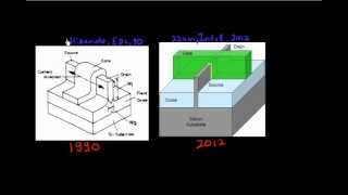
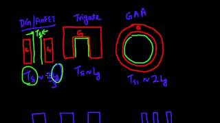
GAAFETs emerge as a key technology in semiconductor design, addressing limitations faced by traditional FinFETs, particularly as devices approach the 3nm node and below. The GAAFET structure features nanowires or nanosheets surrounded completely by the gate material, which significantly enhances electrostatic control over the channel. This control is crucial for managing short-channel effects that are more prominent as transistor dimensions shrink.
Features of GAAFETs
- Superior Gate Control: Due to the all-around gate configuration, GAAFETs can manage the channel more effectively than FinFETs, allowing for higher performance at smaller sizes.
- Completely Surrounded Channels: The nanostructured channel enhances the ability to regulate current flow, improving overall transistor performance.
Importance in Future Semiconductor Devices
GAAFETs are not just a substitute for FinFETs but represent a leap in design philosophy aiming to overcome the scaling challenges faced in modern electronics. As industry standards push for power efficiency and performance, GAAFETs are positioned as essential for continuing advancements in logic and memory technologies.
Youtube Videos

Audio Book
Dive deep into the subject with an immersive audiobook experience.
Introduction to GAAFETs
Chapter 1 of 2
🔒 Unlock Audio Chapter
Sign up and enroll to access the full audio experience
Chapter Content
● Replaces the fin with nanowires or nanosheets completely surrounded by the gate.
Detailed Explanation
GAAFETs are a new type of transistor that improve performance by utilizing structures like nanowires or nanosheets. Unlike traditional FinFETs that have a fin structure with some limitations, GAAFETs are designed such that the channel (the part where current flows) is enclosed all around by the gate. This design allows for better control over the electrical signals, leading to improved efficiency and performance.
Examples & Analogies
Think of GAAFETs as a well-wrapped package of candy. If the candy is wrapped tightly all around, it stays fresh and is less likely to get damaged. Similarly, by surrounding the channel fully with the gate, GAAFETs can keep the electrical signals contained and functioning properly, improving their performance.
Advantages of GAAFETs
Chapter 2 of 2
🔒 Unlock Audio Chapter
Sign up and enroll to access the full audio experience
Chapter Content
● Offers superior gate control compared to FinFETs.
Detailed Explanation
GAAFETs provide much better gate control than FinFETs, which is critical as transistors get smaller. The superior control comes from having the gate surround the channel completely, reducing leakage currents and allowing for more precise switching. This results in lower power consumption and increased data processing speeds, which are essential for advanced computing applications.
Examples & Analogies
Imagine a sports coach who can see all players from every angle on the field. This allows the coach to make better decisions and improve team performance. In the same way, the complete surrounding of the channel in GAAFETs provides unmatched control over the device, enhancing its overall efficiency.
Key Concepts
-
Gate-All-Around FETs: A novel transistor design offering enhanced control.
-
Electrostatic control: Key to managing transistor performance and scaling.
-
Nanostructures: Critical for advancing semiconductor technology.
Examples & Applications
GAAFETs can improve performance in mobile devices requiring compact and power-efficient chips.
The design principles of GAAFETs are paving paths for processors that can handle quantum computing tasks more effectively.
Memory Aids
Interactive tools to help you remember key concepts
Rhymes
When a gate surrounds the wire, it's GAAFET's power that we desire!
Stories
Imagine a castle walls completely encircling a treasure, protecting and controlling access. This is akin to how a GAAFET gate surrounds its channel.
Memory Tools
GO GAAFET! - Gate (all around), Nanosheet (enhances control), Better (performance).
Acronyms
GAAFET
- Gate
- All
- Around
- FET.
Flash Cards
Glossary
- GAAFET
Gate-All-Around FET, a type of transistor with a channel completely surrounded by the gate for better electrostatic control.
- Electrostatic Control
The ability to manage electric fields within a semiconductor device to maintain performance and reduce interference.
- Shortchannel Effects
Performance issues in transistors that occur as the channel length approaches a few nanometers, leading to leakage currents and reduced control over the channel.
Reference links
Supplementary resources to enhance your learning experience.