
Case Study 1: FPGA-Based Digital System Design
Interactive Audio Lesson
Listen to a student-teacher conversation explaining the topic in a relatable way.
Overview of FPGA-Based Systems
🔒 Unlock Audio Lesson
Sign up and enroll to listen to this audio lesson

Today we'll examine FPGA-based systems, which are incredibly useful in creating custom digital designs. Can anyone tell me what an FPGA stands for?

Field-Programmable Gate Array!
Excellent! FPGAs are versatile because we can program them after manufacturing. How do you think this flexibility benefits us in system design?

It allows for testing and modifications without needing new hardware?
Exactly! We can prototype designs quickly and make changes as needed. Now, what about the communication protocols in FPGA designs? Why would we need custom protocols?

To meet specific requirements for different applications?
Yes! Custom protocols can optimize performance for tasks like wireless communication.
In summary, FPGAs provide flexibility, and custom communication protocols enhance data handling efficiency.
Design Challenges in FPGA Implementation
🔒 Unlock Audio Lesson
Sign up and enroll to listen to this audio lesson

As we design FPGA systems, we encounter various challenges. Can anyone name a couple of these challenges?

Timing closure and efficient resource use?
Correct! Timing closure ensures all signals meet their timing requirements; how do we achieve that?
We use static timing analysis to ensure everything is on track?
Exactly! And about resource utilization—why is it important?
To make sure we don’t run out of logic blocks or pins during design?
Right again! Efficient use of FPGA resources can affect overall performance. Lastly, how about error detection in communication protocols?
It helps maintain data integrity, especially over unreliable channels!
Excellent summary! Data integrity is crucial in any communication system, especially wireless. Great work!
Implementing Communication Protocols
🔒 Unlock Audio Lesson
Sign up and enroll to listen to this audio lesson
Let’s discuss implementing a robust communication protocol. What steps do you think we should follow?
First, we would define the protocol specifications.
Good start! What would come next?
Then design the hardware architecture that supports it?
Exactly, and testing is vital too! What methods could we employ for testing the protocol?
Simulation followed by hardware testing on the FPGA?
Correct! These steps help us fine-tune the design before final implementation. Remember, rigorous testing is key in any design process.
Introduction & Overview
Read summaries of the section's main ideas at different levels of detail.
Quick Overview
Standard
In this section, we delve into a case study of designing an FPGA-based custom communication protocol for a wireless sensor network. Key design challenges include achieving timing closure and effective use of FPGA resources, alongside implementing robust error detection and correction mechanisms.
Detailed
FPGA-Based Digital System Design
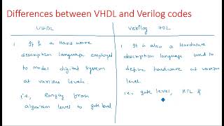
This case study examines the design of an FPGA-based communication system using either VHDL or Verilog. The project targets creating a custom communication protocol for a wireless sensor network, essential for efficient data transmission and reception in embedded systems.
Design Challenges:
- Timing Closure: Ensuring the completion of all required signals within a predefined time frame is critical for optimal operation and reliability.
- Resource Utilization: Efficiently utilizing the FPGA resources, which include configurable logic blocks and input/output pins, to ensure that the design is both optimal and effective in performance.
- Error Detection and Correction: Implementing mechanisms that allow the system to detect and correct errors in data transmission, ensuring data integrity over unreliable wireless communication links.
Design Solution:
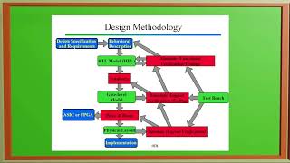
Using either VHDL or Verilog, the construction of a robust communication system is undertaken, adhering to the specified requirements and ensuring efficient performance on an FPGA platform. This involves rigorous testing and validation to meet the operational specifications, ensuring that the system functions as intended.
Youtube Videos

Audio Book
Dive deep into the subject with an immersive audiobook experience.
Introduction to the Case Study
Chapter 1 of 3
🔒 Unlock Audio Chapter
Sign up and enroll to access the full audio experience
Chapter Content
A case study of designing an FPGA-based system using VHDL or Verilog. The project involves designing a custom communication protocol for a wireless sensor network.
Detailed Explanation
This chunk introduces the case study, focusing on an FPGA-based system design. The main task is to create a custom communication protocol used in a wireless sensor network. This means building a set of rules and processes that devices in a sensor network will use to communicate effectively with each other.
Examples & Analogies
Consider this like creating a new language for a group of people to use so they can share information safely and effectively. Just as people need to agree on grammar and vocabulary, the devices need a custom protocol to ensure they understand each other.
Design Challenges
Chapter 2 of 3
🔒 Unlock Audio Chapter
Sign up and enroll to access the full audio experience
Chapter Content
● Design Challenges:
○ Timing closure and efficient use of FPGA resources.
○ Implementing error detection and correction mechanisms in the communication protocol.
Detailed Explanation
This chunk outlines key challenges that need to be addressed in the design process. 'Timing closure' refers to ensuring that signals in the FPGA circuit reach their destination within required time limits to maintain functionality. 'Efficient use of FPGA resources' means that the design must maximize the utilization of the available hardware resources without wasting them. Additionally, implementing error detection and correction mechanisms ensures that any errors in the communication signals can be identified and corrected, maintaining the reliability of the communication protocol.
Examples & Analogies
You can think of timing closure like making sure that a relay race team passes the baton quickly enough without dropping it. Just as runners need to time their movements, the FPGA components need to synchronize their operations. Moreover, adding error detection is like having a coach who watches for dropped batons and can quickly help the team recover.
Design Solution
Chapter 3 of 3
🔒 Unlock Audio Chapter
Sign up and enroll to access the full audio experience
Chapter Content
● Design Solution:
Using VHDL or Verilog, implement a robust communication system that meets the required specifications and performs efficiently on an FPGA.
Detailed Explanation
This chunk describes the proposed solution for overcoming the design challenges listed previously. The approach involves using either VHDL or Verilog, which are hardware description languages, to build a communication system that adheres to defined specifications while ensuring efficient performance. It implies that the designers will program the FPGA to create a reliable and functioning prototype of the communication protocol.
Examples & Analogies
Imagine you are assembling a complex puzzle. Using VHDL or Verilog is like using a clear picture as a guide, allowing you to fit the pieces (FPGA resources) together to create a complete and working communication system. The goal is to ensure that all pieces fit well to represent the final design accurately.
Key Concepts
-
FPGA: A device that offers flexibility in digital circuit design.
-
Communication Protocol: It dictates how devices communicate over a network.
-
Timing Closure: It's essential to ensure circuit signals meet timing specs, critical for performance.
-
Error Detection: A necessary component in communication protocols to maintain data integrity.
Examples & Applications
Designing a custom communication protocol for sensor data transmission in an FPGA-based IoT device.
Implementing error correction techniques such as Hamming codes in an FPGA communication system.
Memory Aids
Interactive tools to help you remember key concepts
Rhymes
To keep data clear and bright, detection is a must, day and night!
Stories
Imagine a messenger in a village delivering messages. To ensure they arrive intact, he checks each message for errors before sending it, just like error detection in protocols!
Memory Tools
When remembering FPGA: Think 'Flexibility, Programmable, Gate, Array'. Each letter stands for an essential aspect.
Acronyms
Use FRESH to remember
'FPGA Resource Efficiency and Signal Handling'.
Flash Cards
Glossary
- FPGA
Field-Programmable Gate Array, an integrated circuit that can be programmed after manufacturing.
- Communication Protocol
A set of rules and conventions for data transmission between devices.
- Data Integrity
The accuracy and consistency of data over its lifecycle.
- Timing Closure
The process of ensuring that all signals in a circuit meet timing requirements.
- Resource Utilization
The efficient use of available logic blocks and I/O pins within an FPGA.
- Error Detection and Correction
Techniques used to identify and rectify errors in data transmission.
Reference links
Supplementary resources to enhance your learning experience.