
Verilog in FPGA and ASIC Design
Interactive Audio Lesson
Listen to a student-teacher conversation explaining the topic in a relatable way.
Introduction to Verilog in FPGA Design
🔒 Unlock Audio Lesson
Sign up and enroll to listen to this audio lesson

Today, we're diving into how Verilog is utilized in FPGA design. Can anyone tell me why efficient resource usage is crucial?

I think it's because FPGAs have limited resources, so we need to make the most of them?
Exactly! Efficient resource usage helps in optimizing the design and ensuring we can fit our entire logic onto the FPGA. Can anyone think of a specific resource we should optimize?

What about I/O pins? They are limited, right?
That's right! I/O pins are critical, and optimizing their use can significantly enhance performance.
Remember this acronym: R.U.P - Resource Utilization Planning. Let's keep that in mind!

How about synchronization issues when dealing with clock domains?
Good point! Synchronization ensures that signals are communicated correctly within the system. Can anyone explain what could happen if we neglect synchronization?

We might get timing issues leading to incorrect output?
Absolutely! Timing issues can severely affect functionality, especially in complex systems.
To summarize, in Verilog for FPGA design we focus on Resource Utilization Planning and synchronization to ensure smooth operation and optimal performance.
Project Example of a 16-bit Parallel Adder
🔒 Unlock Audio Lesson
Sign up and enroll to listen to this audio lesson

Now let’s talk about the project example: designing a 16-bit parallel adder using Verilog. What do you think would be the first step in this project?
I think we need to define the inputs and outputs first.
Correct! Start by defining inputs like two 16-bit numbers and an output for the sum. What sort of design considerations should we keep in mind?
We should ensure that it meets timing constraints.
Exactly! Timing constraints are vital. We also need to simulate our design first to verify its functionality. What simulation tools can we use?
ModelSim or XSIM?
Yes! ModelSim and XSIM are great choices for simulating our Verilog designs. In summary, when working on our 16-bit adder, we need to focus on defining inputs, ensuring timing constraints, and utilizing simulation tools efficiently.
Introduction & Overview
Read summaries of the section's main ideas at different levels of detail.
Quick Overview
Standard
Verilog plays a crucial role in FPGA and ASIC design, offering concise syntax and powerful simulation capabilities. This section emphasizes resource efficiency, clock domain modeling, and provides project examples to demonstrate effective design practices.
Detailed
Verilog in FPGA and ASIC Design
Overview
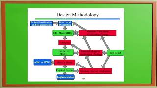
This section delves into the pivotal role of Verilog as a hardware description language in the design of both Field-Programmable Gate Arrays (FPGAs) and Application-Specific Integrated Circuits (ASICs). It underscores the language's concise syntax and robust simulation capabilities, making it a favored choice among engineers.
Design Considerations
- Efficient Resource Usage: When designing for FPGAs, there is a significant emphasis on maximizing the efficient use of hardware resources such as logic blocks and I/O pins. This involves making strategic design choices that enhance performance while conserving resources.
- Clock Domains and Synchronization: Correctly modeling clock domains and ensuring synchronization is critical, especially in complex systems. This aspect guarantees that various components communicate effectively, minimizing timing issues.
Practical Project Example
- 16-bit Parallel Adder Design: A practical application of Verilog involves designing a 16-bit parallel adder to be implemented on an FPGA. This example serves to illustrate design techniques that prioritize proper timing constraints and overall performance verification.
In summary, Verilog is integral to efficient FPGA and ASIC designs, combining concise language features with powerful simulation tools, thereby enhancing the development of complex digital systems.
Youtube Videos

Audio Book
Dive deep into the subject with an immersive audiobook experience.
Overview of Verilog in FPGA and ASIC Design
Chapter 1 of 3
🔒 Unlock Audio Chapter
Sign up and enroll to access the full audio experience
Chapter Content
Verilog is used in both FPGA design and ASIC development due to its concise syntax and powerful simulation capabilities.
Detailed Explanation
Verilog is a hardware description language that allows designers to describe the behavior and structure of electronic systems efficiently. Its concise syntax means designers can write less code to achieve the same functionality, making it quicker to develop designs. Additionally, Verilog excels in simulating these designs, allowing engineers to test their functionality before they are implemented in hardware. This simulation capability is crucial as it helps identify and fix errors early in the design process, ultimately saving time and resources.
Examples & Analogies
Imagine you're writing a recipe. A concise recipe gives you just the essential steps without unnecessary details; this makes it quicker to prepare a meal. Similarly, Verilog provides a streamlined way for engineers to build digital systems, allowing them to focus on the essential elements of the design without getting bogged down by verbosity.
Design Considerations for Verilog in FPGA and ASIC Projects
Chapter 2 of 3
🔒 Unlock Audio Chapter
Sign up and enroll to access the full audio experience
Chapter Content
● Design Considerations:
- Focus on efficient resource usage, especially when working with FPGA hardware.
- Correctly model clock domains and synchronization when designing complex systems.
Detailed Explanation
When using Verilog for FPGA and ASIC design, it's crucial to use resources effectively. For FPGAs, this means optimizing how logic blocks and pins are used to prevent wasting valuable hardware resources. Moreover, designing complex systems often involves multiple clock domains, which are different frequency signals that need to operate correctly together. Properly modeling these clock domains ensures that data is synchronized accurately across the system, preventing timing issues that could lead to malfunction.
Examples & Analogies
Think of designing a traffic system in a city with various traffic lights (different clock domains). If each light operates on a different schedule but they aren’t coordinated, it can lead to confusion and traffic jams. Similarly, in digital design, if clock domains are not properly synchronized, it leads to errors and breakdowns in communication between different parts of the system.
Project Work Example: 16-Bit Parallel Adder
Chapter 3 of 3
🔒 Unlock Audio Chapter
Sign up and enroll to access the full audio experience
Chapter Content
● Project Work Example:
- Design a 16-bit parallel adder in Verilog and implement it on an FPGA. Ensure proper timing constraints and verify performance.
Detailed Explanation
Designing a 16-bit parallel adder involves creating a circuit that can add two 16-bit binary numbers simultaneously and produce a result. When implementing this adder in Verilog on an FPGA, the designer must ensure that the logic created fits within the FPGA's hardware limits. Additionally, verifying performance involves checking that the adder operates correctly at the intended speed and meets any timing requirements, which are critical for ensuring that the addition completes in the required time frame.
Examples & Analogies
Consider a race where two cars (the 16-bit numbers) are simultaneously driving towards a finish line (the result of the addition). Just like in racing, both cars need to reach the finish line quickly and without any issues, which translates to ensuring the adder works efficiently and correctly. If one car (one part of the circuit) lags because of timing issues, the results will be erroneous, which is unacceptable in a competitive race, just as in digital design.
Key Concepts
-
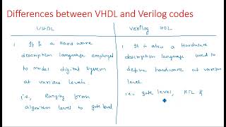
Concise Syntax of Verilog: Verilog's compact syntax makes it easier to write and debug code than VHDL.
-
Efficient Resource Usage: Optimizing the use of hardware resources in design is critical for performance.
-
Clock Domain Modeling: Properly managing clock domains is essential in complex system design.
-
Simulation Capabilities: Verilog provides powerful simulation tools that are vital for validating designs.
Examples & Applications
A simple implementation of a 16-bit parallel adder in Verilog can demonstrate the language's capability to handle complex arithmetic operations.
Using Verilog to design a shift register helps illustrate how efficient resource usage can be managed in an FPGA.
Memory Aids
Interactive tools to help you remember key concepts
Rhymes
For a data flow that won’t stutter, keep your clocks in sync, don’t let them utter!
Stories
Imagine you are a conductor of an orchestra. Each musician must play in sync—just like components in a circuit must synchronize their clock signals to avoid delays.
Memory Tools
To remember Resource Utilization Planning, think R.U.P—like 'Rup' a friend who efficiently organizes your resources.
Acronyms
CSD - Clock Synchronization Discipline. Always make sure each clock is in harmony.
Flash Cards
Glossary
- FPGA
Field-Programmable Gate Array, a type of hardware that can be configured by the customer or designer after manufacturing.
- ASIC
Application-Specific Integrated Circuit, a chip designed for a specific application, rather than for general-purpose use.
- Clock Domain
A region in a circuit that is driven by a single clock signal.
- Timing Constraints
The specification of time requirements within which the signals must meet and achieve the desired behavior.
- Simulation
The process of using a model to predict the behavior of a design before implementation.
Reference links
Supplementary resources to enhance your learning experience.